The Semiconductor Industry
A description of the innerworkings of the semiconductor Industry
IN-DEPTH ANALYSISSEMICONDUCTORINDUSTRY
Rafael CARRARA
4/7/202631 min read
Semiconductor industry - 2025
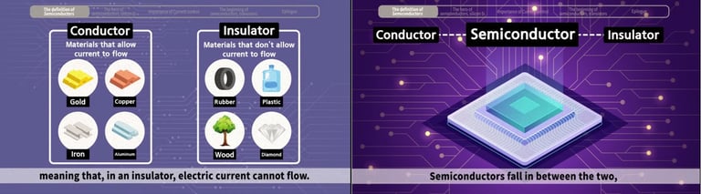
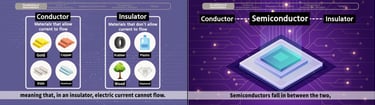
What is a semiconductor?
By definition a semiconductor refers to a material that sits between a conductor and an insulator. Conductors such as gold, copper, iron and aluminum are materials that allow electricity to flow. Insulators such as rubber, plastic, wood and diamonds resist electricity, meaning that in an insulator electric current cannot flow. Semiconductors fall in between the two, which means that semiconductors sometimes have electrical conductivity and sometimes don't.
By artificially adding impurities into a semiconductor, you can control the flow of current.
How is a Semiconductor Created?
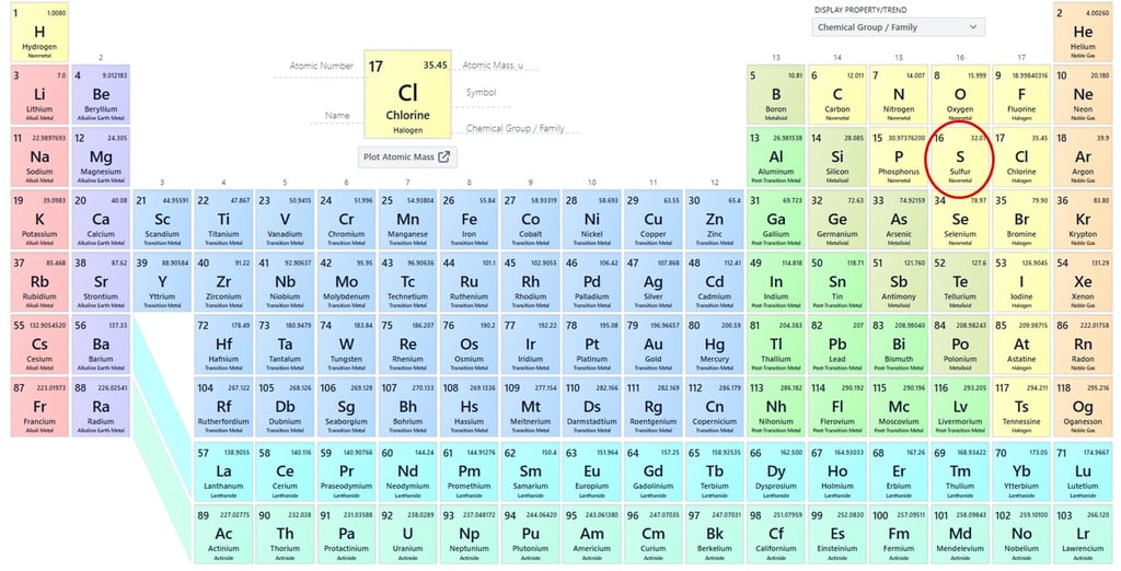
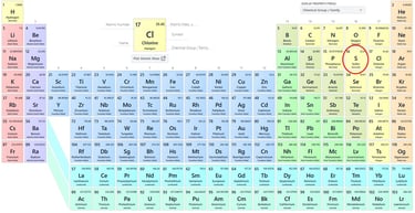
The starting point is an element called silicon. Does the term silicon sound familiar ?
Yes, you are correct if you thought of the Silicon Valley the high-tech IT research complex in the US. The name of this place came from Silicon, an element in semiconductors. Silicon does not only represent the element but also symbolically represents the high-tech industry. Returning to our main point silicon is also the 14th element of the periodic table just below carbon. It's easily found in sand soil or rocks and it makes up almost 28 percent of the Earth's crust being the second most abundant element after oxygen.
Though elements like germanium and gallium arsenide can still be used.
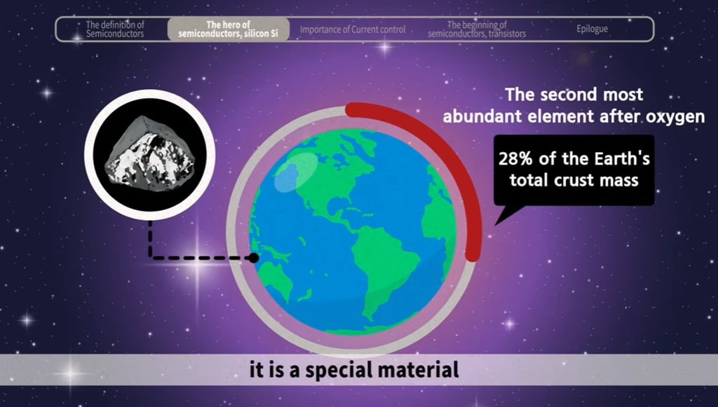

it is a special material and also a very common material at the same time: silicon crystal has low electric conductivity and high resistance. Therefore, by adding impurities into it, you can make it have or not have current flow.
You can see in the following link some of the physics behind this : https://www.micron.com/content/dam/micron/educatorhub/device-physics/semiconductor-fundamentals/micron-semiconductor-fundamentals-and-pn-junction-device-physics-presentation.pdf
Why is the presence or absence of electrical conductivity important ?
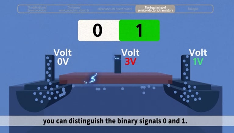
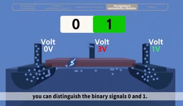
This is because semiconductors are used in digital devices. Semiconductors process all kinds of information using binary numbers the simple zero and one utilizing this you can control the current flow through converting it to a digital language of zeros and ones. Using this we can control electronic devices and make them remember information.
what was the world's first semiconductor ?
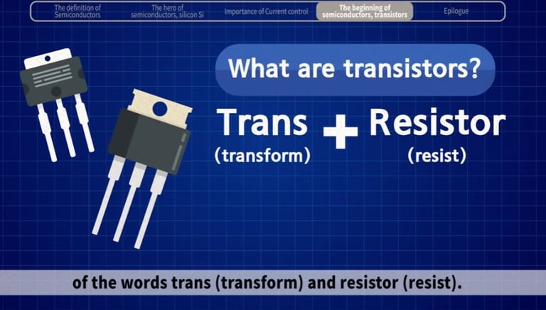
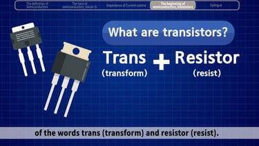
It was a transistor: In 1947 Bell Labs in the United States invented the world's first transistor, and from there the modern history of semiconductors began. The word transistor is a combination of the word “trans” and “resistor”.

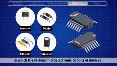
It's the part that is in charge of amplifying and switching electrons in an electronic circuit through the switching function of the transistor. You can distinguish the binary signals zero and one and a semiconductor chip which is the Assembly of countless transistors is able to store information and perform operation just as how the brain functions.
By arranging transistors in intricate patterns, they realized they could selectively guide current along a path of their choosing and make it do some useful work along the way.
Later as the integrated circuit or IC was developed by Jack Kilby in 1958 the shape of today's semiconductors was created :

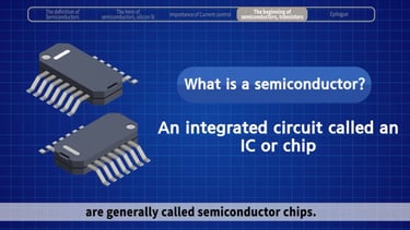
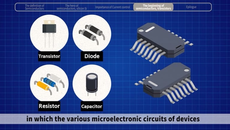
Billions of transistors lie inside a chip as small as a fingernail with multiple transistors, diodes, resistors, and capacitors in which the various microelectronic circuits of devices are attached into one chip. Also the more transistors a chip has, the higher its computing power :
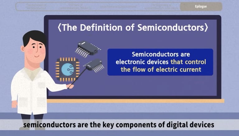
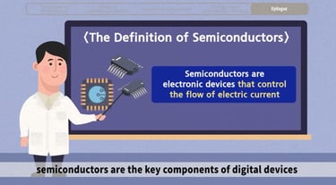
in summary semiconductors are the key components of digital devices that change resistivity depending on an applied electric field
To conclude :
Semiconductors are the key components of digital devices that change resistivity depending on an applied electric field :
What are semiconductors used for?
Semiconductors are essential for manufacturing chips, integrated circuits, and microprocessors.
When we talk about the semiconductor market, we mainly refer to the market for the final product: the chip.
We need processors for a vast range of devices, including computers, smartphones, cars, servers, video games, medical and industrial machines, and even weapons. Semiconductors are the cornerstone of modern life. Le Monde aptly describes their importance: "Semiconductors are to electronics what oil is to industry."
For example, a car requires more than 1,000 electronic chips—and even more for hybrid or fully electric vehicles.
It is in every electrical element, and is critical for the functioning of modern society.
Due to their omnipresence, the semiconductor market is enormous, valued at over $611 billion in 2024, according to The Semiconductor Industry Association (SIA).
The market is projected to exceed $700 billion in 2025, driven primarily by AI demand. By 2030, the industry is expected to surpass $1 trillion (source: McKinsey, SIA, SEMI).
Of course, we can’t talk semiconductors without talking about AI that pushes the demand of semiconductors.
By misuse of language, semiconductors are often confused with chips (which are made from semiconductors).
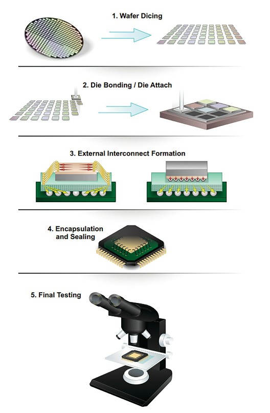
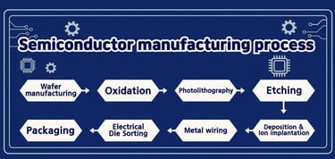
What is actually the process to make Chips ?
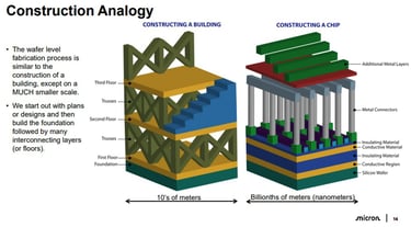
The production of a wafer is a lot like the production of a building :

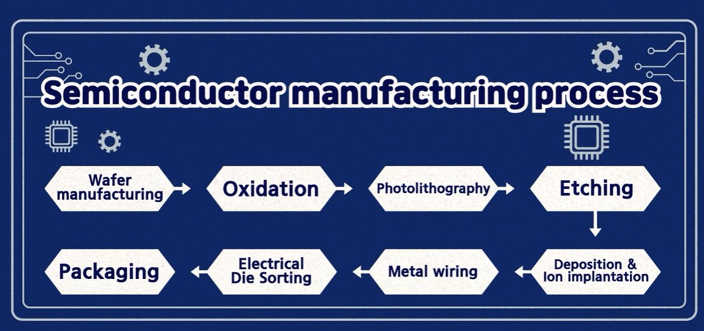
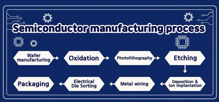
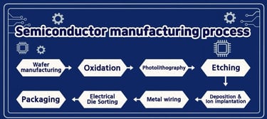
The production process is divided into 8 main stages :
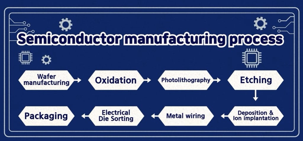
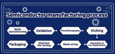
let's take a closer look at these processes :
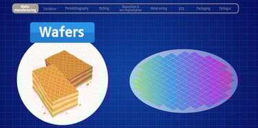
1) Wafer Manufacturing
Semiconductors are stacked high and solid to form a complex structure similar to a high-rise building. Constructing a building starts with the foundation. A wafer is the foundation for the semiconductor.
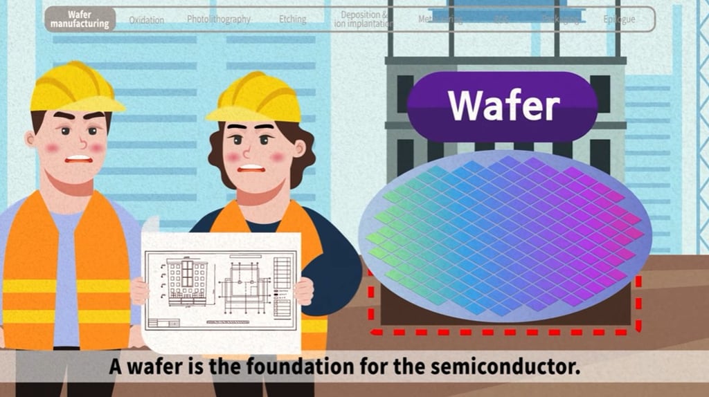

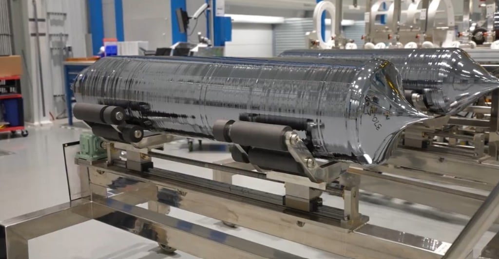
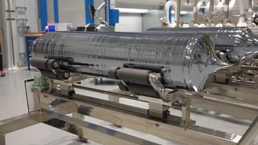
Most wafers are made of silicon extracted from sand. How can these tiny grains of sand become a wafer ?
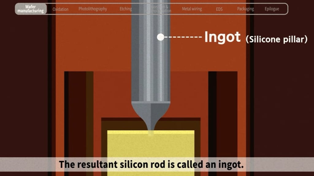
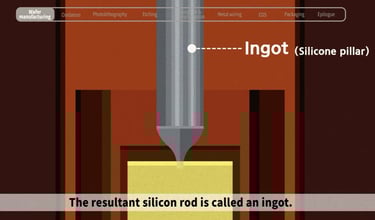
First sand is heated until it melts into a high purity liquid and then gets solidified by crystallization :


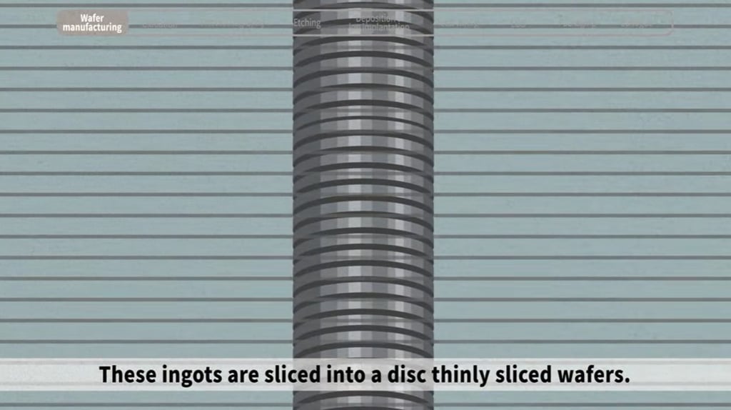
The resultant silicone Rod is called an Ingot :
These ingots are sliced into discs and from those ingots we thus obtain thinly sliced Wafers :

The surface of sliced Wafers is rough and contains defects so polishing machines are used to polish the surface of the wafer :
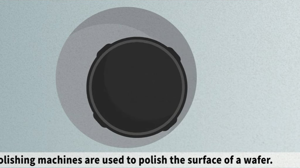

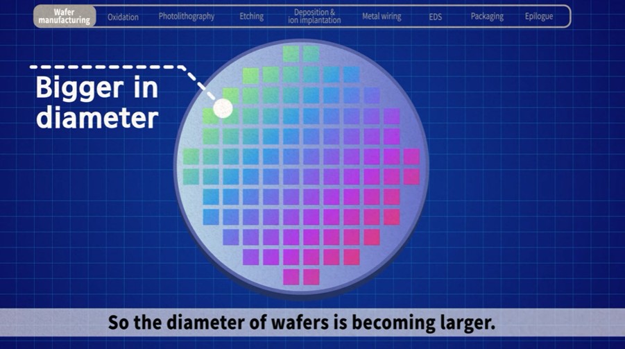
The reason is that defects on the surface could negatively affect the precision of circuits. If you look at a photo of Wafers you can see a grid pattern on the surface. As you might have guessed, the word wafer comes from biscuit Wafers :

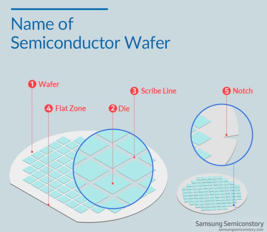
A wafer made this way is the main material for semiconductors because the larger the diameter is the greater the number of chips that can be produced per wafer is. So the diameter of Wafers is becoming larger :

2) Oxidation
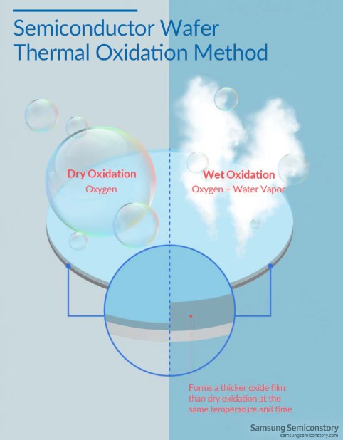
Because the resultant thin disc-shaped wafer is not conductive yet, a process to make wafers semiconductive is required first.
Wafers go through the oxidation process, oxygen or water vapor is sprayed on the wafer surface to form a uniform oxide film. This oxide film, protects the wafer surface during the following processes and also blocks current leakage between circuits. The film acts as a strong protective shield :

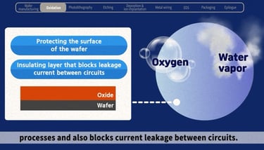

Due to miniaturization, this step is becoming increasingly complex.
3) Photolithography
Now, the foundation is ready. The building up process begins.
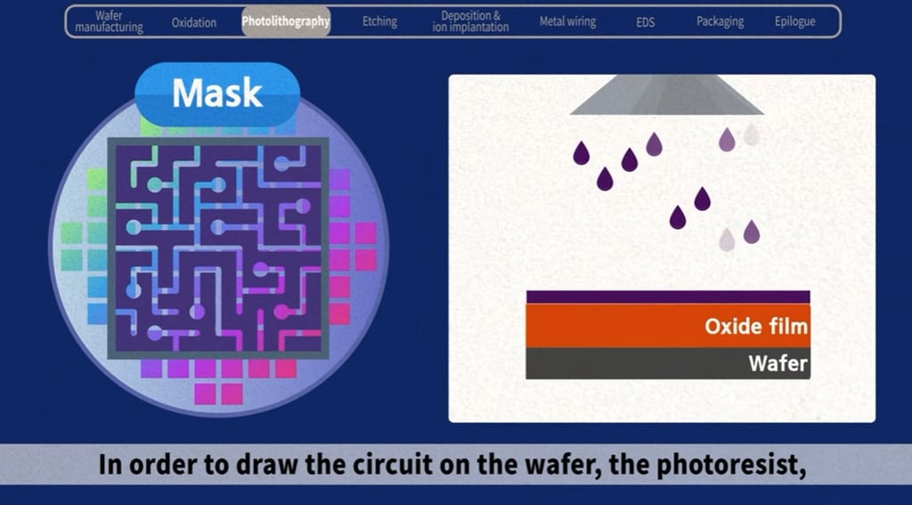
Just as you draw blueprints to build a building, you draw a circuit design onto a wafer which is called the photolithography process.
It is called photo for short, because it is similar to developing a photo taken on a film camera. With semiconductors, a photo mask functions as the film. A photo mask is a glass substrate with a computer designed circuit pattern.
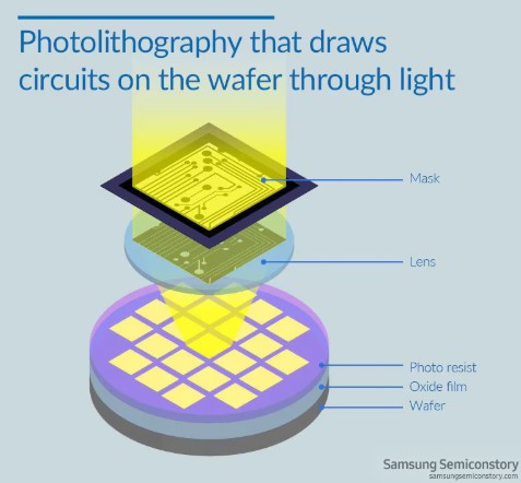

In order to draw the circuit on the wafer, the photoresist, a material that responds to light is applied thinly and evenly on the oxide film previously placed on the wafer :

Now, when light transfers the pattern photo mask the circuit is drawn on the wafer surface, just like developing a photo.
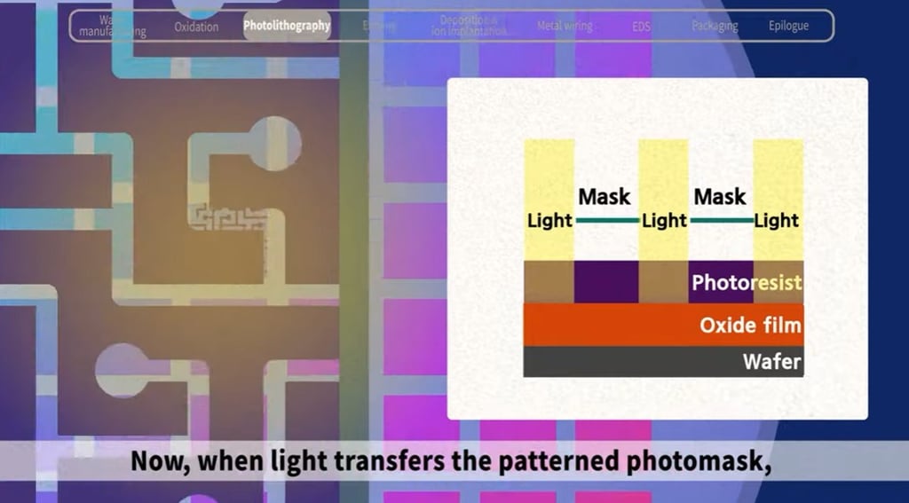

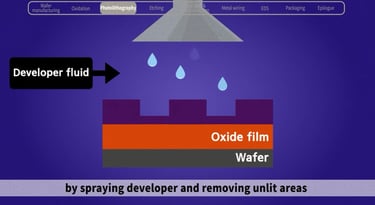
A circuit pattern is imprinted on the wafer by a developer fluid and removing unlit areas from the areas that are exposed to light.
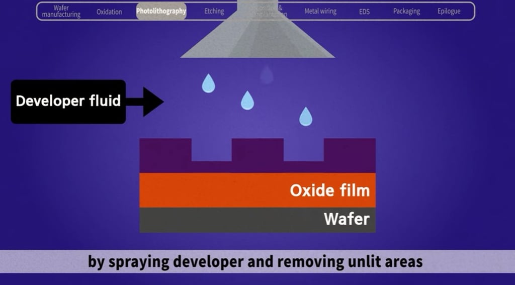
After an inspection of the wafer to check whether the pattern is drawn well, it moves on to the next step.


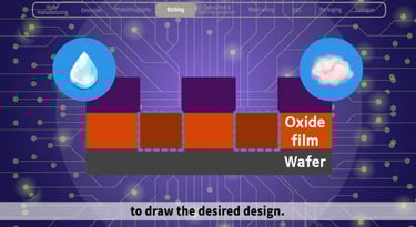
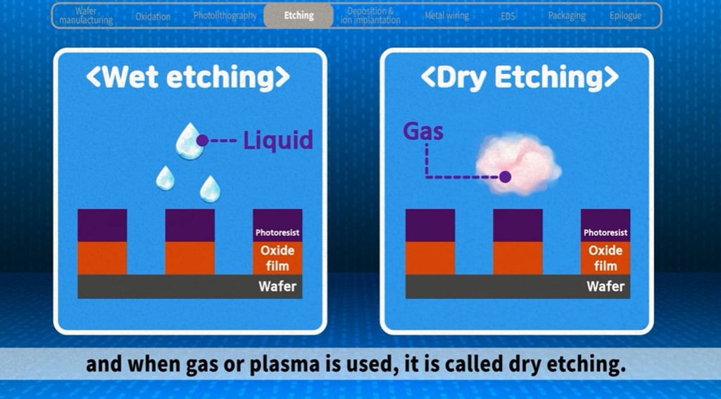
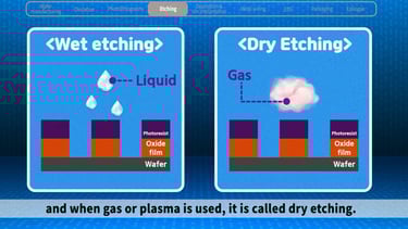
4) Etching
Now, unnecessary materials are carved out so that only the design pattern remains using a liquid or gas etching. Unnecessary materials are selectively removed to draw the desired design.

When chemical solutions are used for etching it is called wet etching and when gas or plasma is used it is called dry etching.
Let’s imagine constructing a building on a semiconductor chip smaller than a fingernail and thinner than a sheet of paper.
The photolithography process and the etching process are repeated several times on the wafer layer by layer.
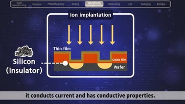
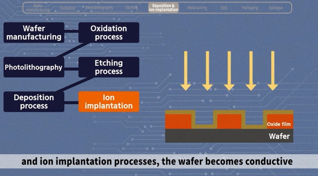
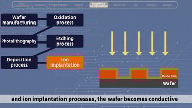
5) Deposition & Ion implantation

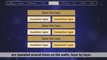
Here an insulating film that separates and protects the stacked circuits is required. It is called a thin film coating.
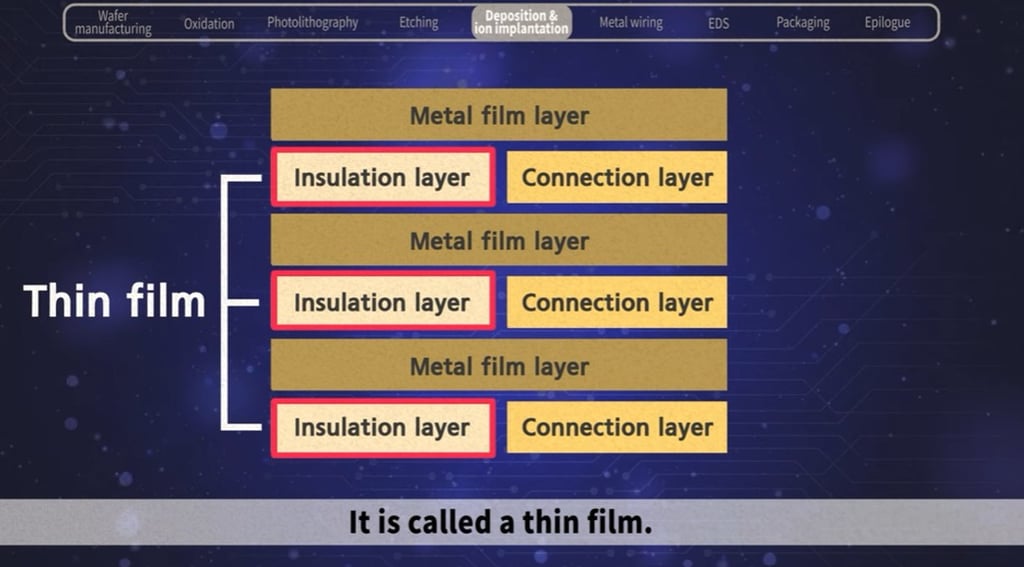
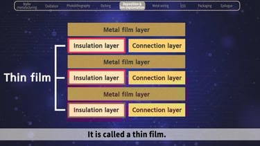
The thin film, at a desired molecular or Atomic level, onto a wafer is called deposition.
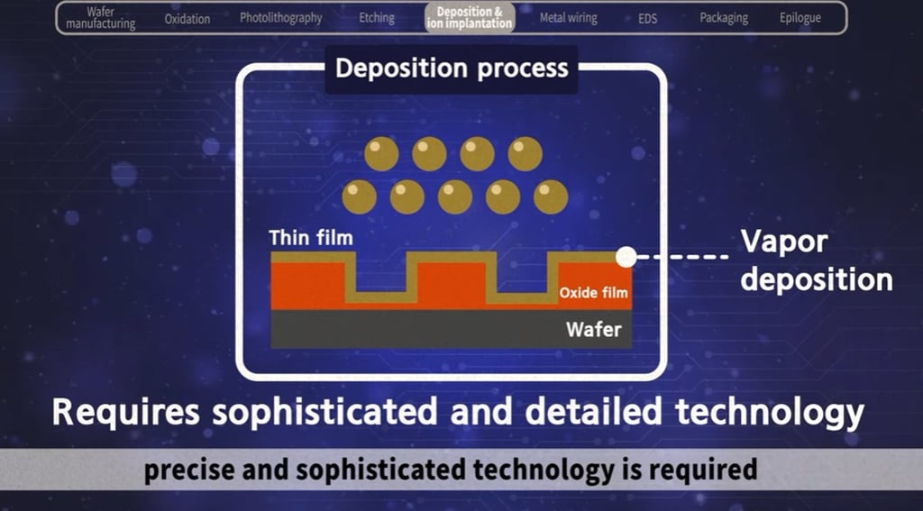

Since the coating is so thin, precise and sophisticated, technology is required to uniformly apply the thin film on a wafer.
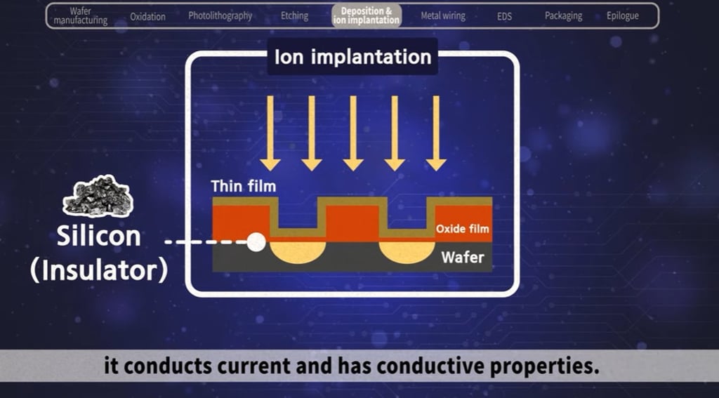
To give the semiconductor electrical characteristics, ion implantation is also required.
A semiconductor made of silicon, does not conduct electricity but by adding impurities, it conducts current and has conductive properties.
In summary, through the wafer manufacturing, oxidation, photolithography, etching, deposition and ion implantation processes, the wafer becomes conductive and numerous circuits are drawn on it.
Here is a link that explains the different types of deposition : https://newsroom.lamresearch.com/Deposition-Essentials-Semi-101?blog=true
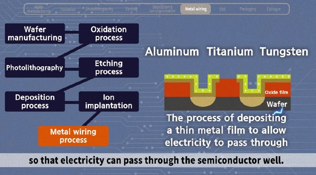
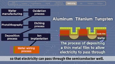
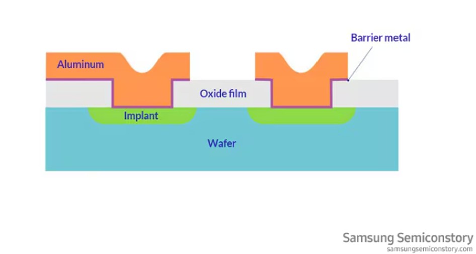
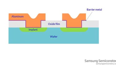
6) Metal Wiring
Now, in order for this circuit to work an electrical signal must be applied: it is necessary to create a path for electricity to pass through according to the Circuit pattern.

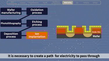
This process is called the metal wiring process. It is a process that allows electricity to flow by depositing a thin metal film using materials such as aluminum, titanium or tungsten so that electricity can pass through the semiconductor.
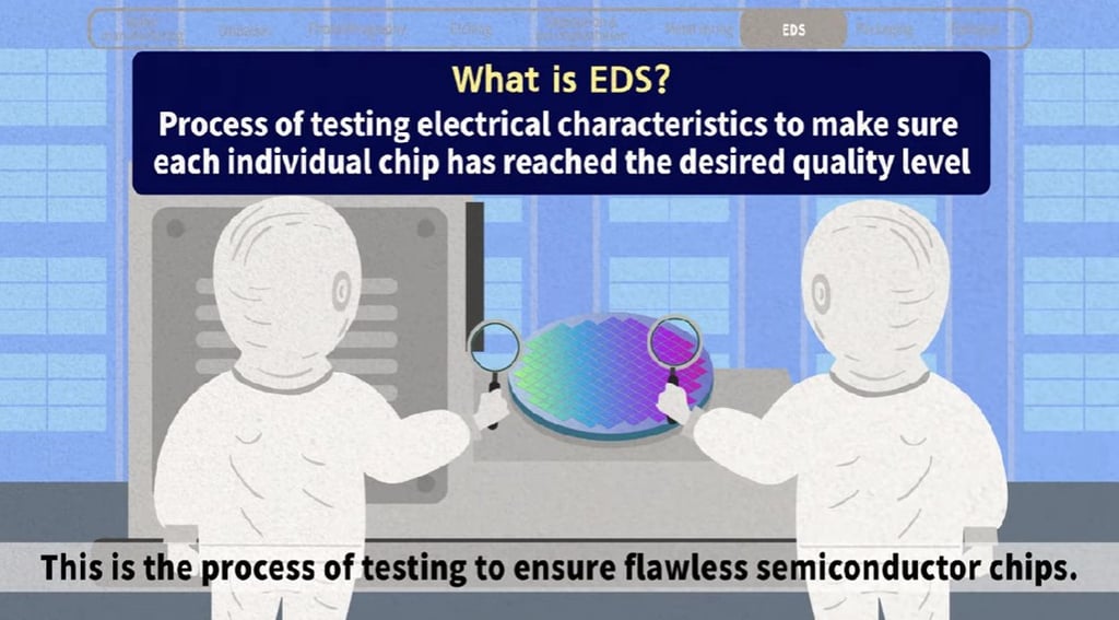
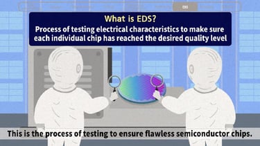
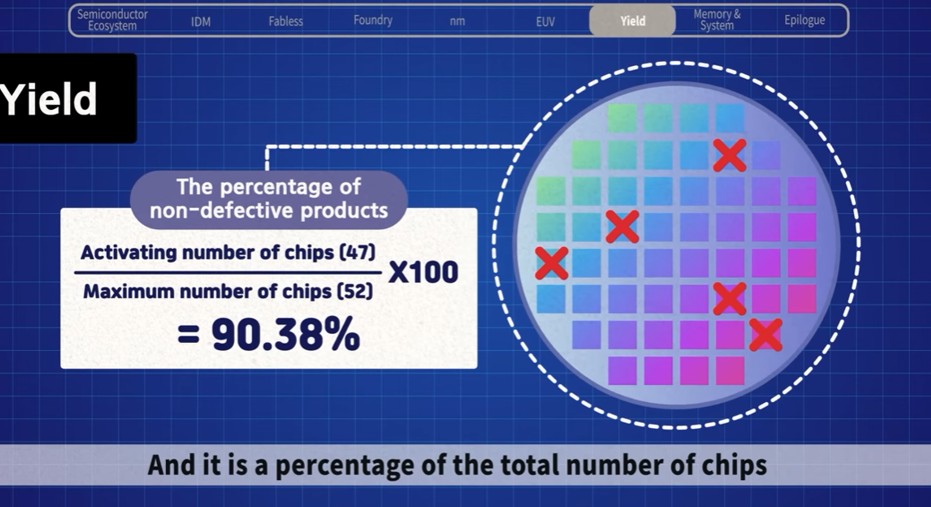
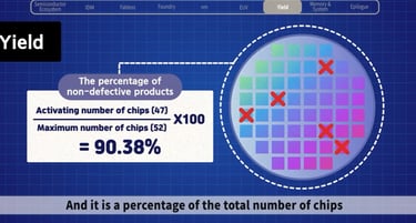
7) Electrical Die Sorting (EDS)
Well, the chip manufacturing processes are now coming toward completion. The next step is EDS. This is the process of testing to ensure flawless semiconductor chips, in other words, it is a testing step to sort out defective chips.
Here is a link if you want more detail on the different steps : https://semiconductor.samsung.com/support/tools-resources/fabrication-process/eight-essential-semiconductor-fabrication-processes-part-8-eds-electrical-die-sorting-for-the-perfect-chips/
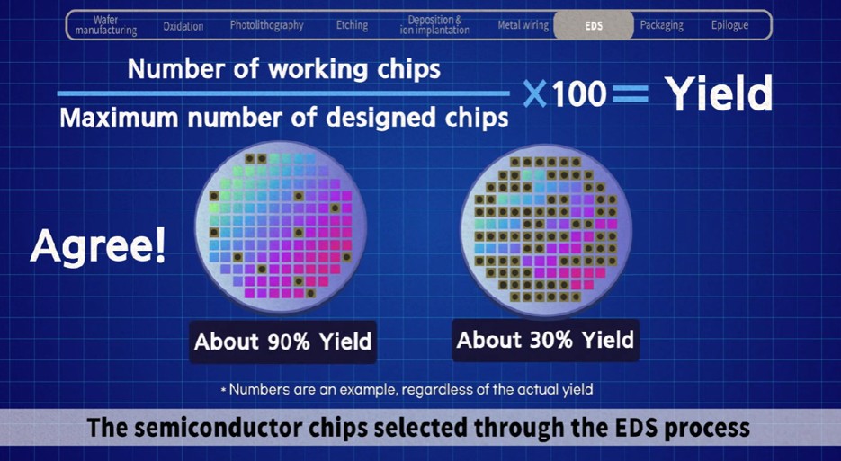
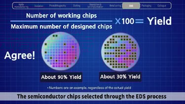
Yield is a percentage of prime chips relative to the maximum chip count on a single wafer. The semiconductor chips selected through the EDS process are made in a form suitable for devices.
Why does yield matter economically? A single 300mm wafer costs thousands of dollars to process through all these steps. If your yield is 80%, you lose 20% of that investment. This is why defect control is obsessive in semiconductor fabs—a single particle of dust can destroy a chip worth hundreds of dollars. Leading-edge chip production takes 3–4 months from wafer start to finished chip, which explains why supply chain disruptions are so devastating.
8) Packaging
This is the last process; the molding finishes the chip package to its desired shape. After sealing the semiconductor and labeling the product name the semiconductor chip we commonly see is completed.
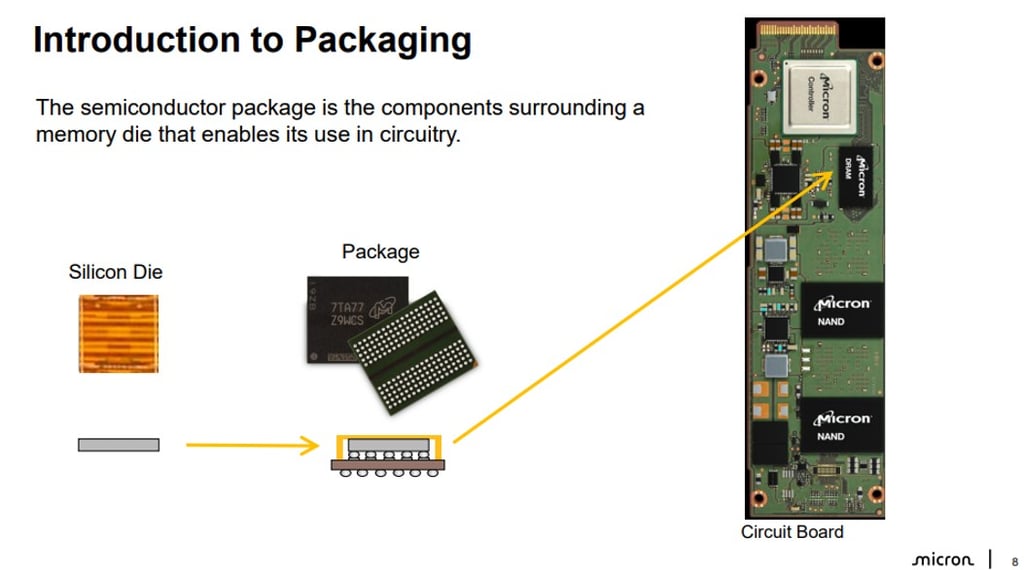

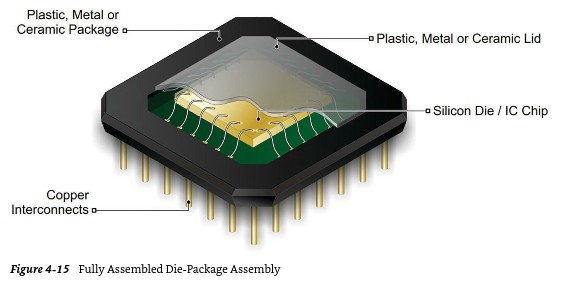
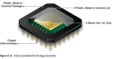
Of course, only after going through the final test will it become a finished product.
If you want to see more detail on each of the steps described below you can click on the following links:
https://semiconductor.samsung.com/support/tools-resources/fabrication-process/eight-essential-semiconductor-fabrication-processes-part-9-packaging-to-protect-the-chips-from-external elements/

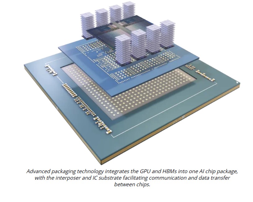
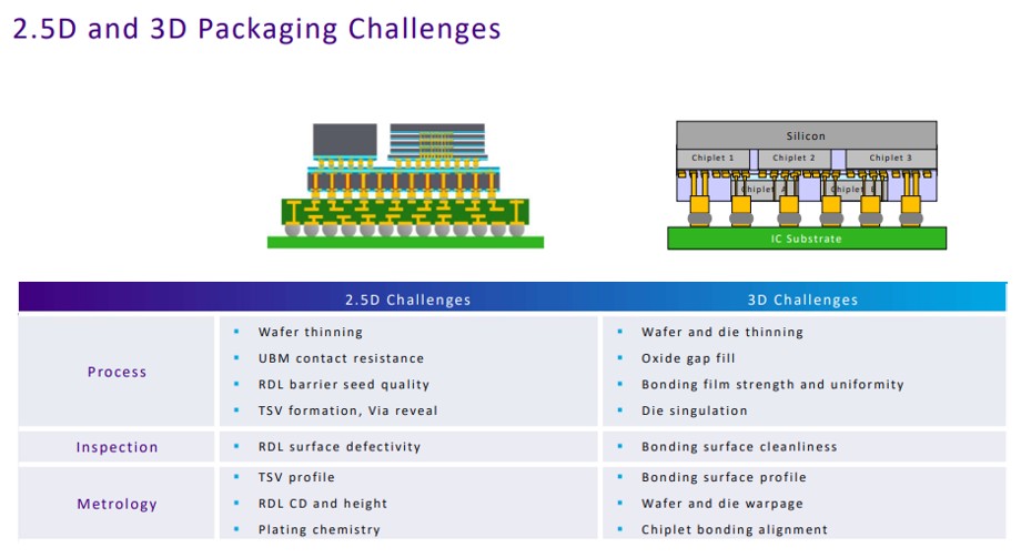
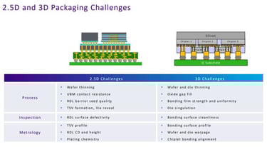
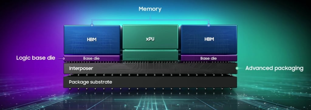
Advanced Packaging — The New Frontier

Traditional packaging places a single chip (die) into a single package. But modern demands, especially for AI, have driven a revolution called advanced packaging. Instead of making one giant monolithic chip, manufacturers now assemble multiple smaller specialized chips (called chiplets) into a single package, like assembling LEGO blocks.

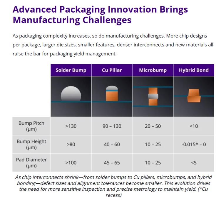
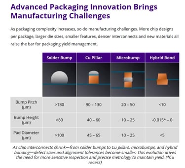
Key advanced packaging technologies include:
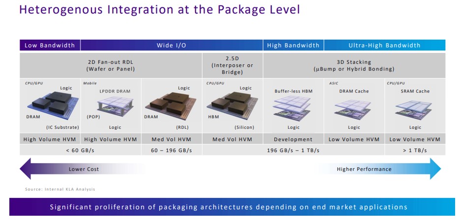
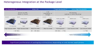
• 2.5D packaging: Chiplets are placed side by side on a silicon interposer (a thin connection layer). This is how Nvidia builds its AI GPUs and AMD builds its EPYC server processors using TSMC’s CoWoS (Chip-on-Wafer-on-Substrate) technology.
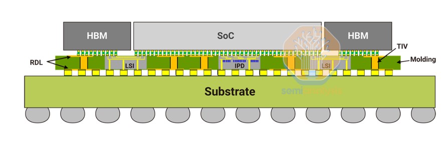
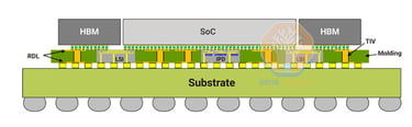
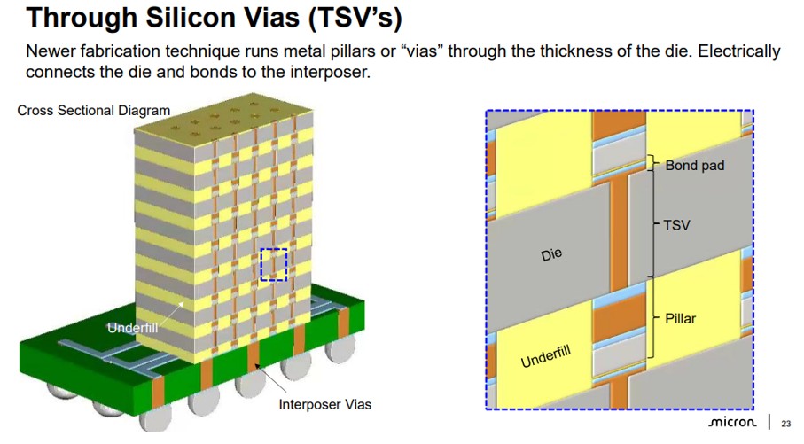
• 3D stacking: Dies are stacked vertically and connected with TSVs (Through-Silicon Vias). HBM (High Bandwidth Memory) uses this approach—multiple DRAM dies stacked on top of each other.
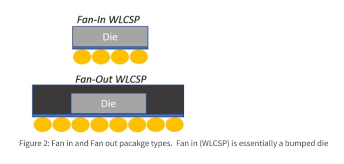
• Fan-Out Wafer-Level Packaging (FOWLP): Used for mobile chips, it eliminates the traditional substrate, making packages thinner and cheaper.

Advanced packaging is now one of the fastest-growing segments of the semiconductor industry. TSMC, Intel, and Samsung are investing billions into packaging capacity.
For a beginner: think of it as the shift from building single-story houses to building skyscrapers.
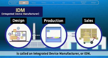
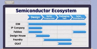
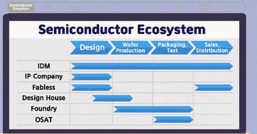
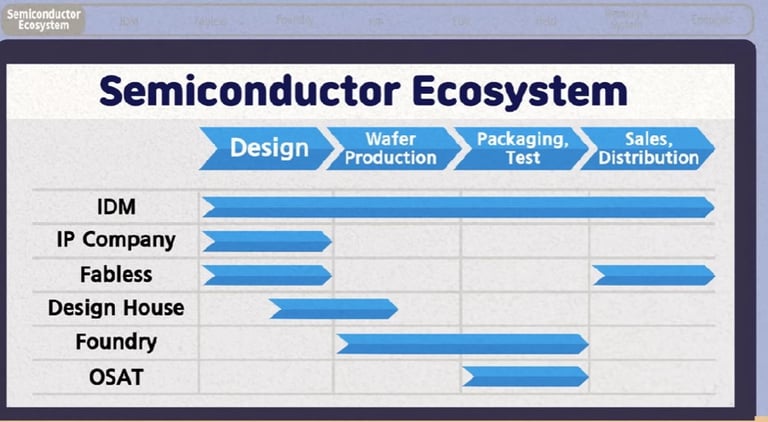
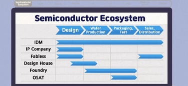
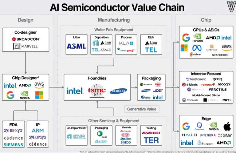
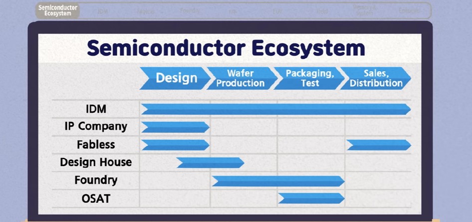
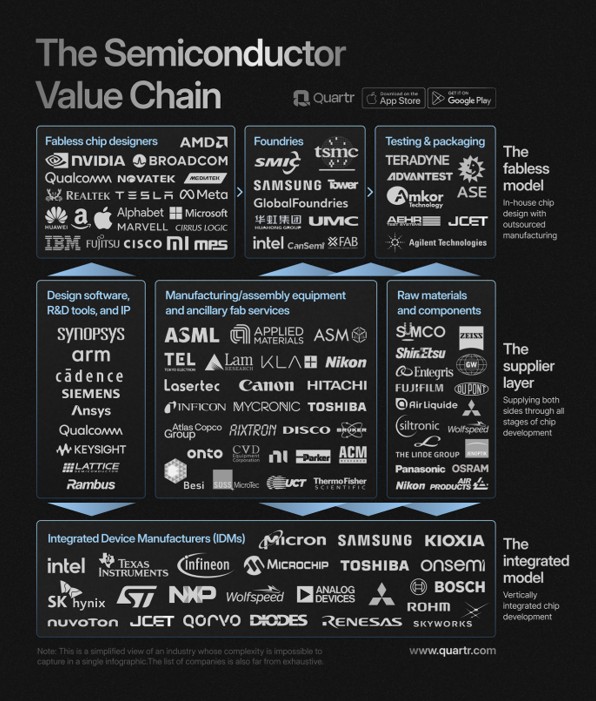
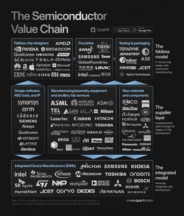
Ecosystem and Value Chain of the Semiconductor Industry
Now that we understand how Chips are made, let’s ask ourselves, What is the ecosystem and the value chain to produce those chips ?
As we have seen previously there are 8 main stages to produces those Chips :
But Production is not the only important part of the Semiconductor industry. You also have Design, Distribution, Inspection and Assembly.
Here is the example of the journey of a smartphone to help you visualize the steps and what the supply chain looks like:
The first step of semiconductor manufacturing is Design. Then Wafers which are produced based on the designs are cut into hundreds of individual chips. The next process is packaging where chips are attached on substrates or electronic devices. When quality inspections finish the final products are ready to be sold the entire process can be handled by one company or multiple companies can work together.
Here are the different categories of companies that are part of that ecosystem :

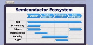
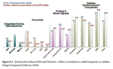
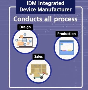
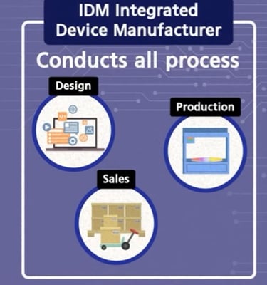
1) IDM – Integrated Device Manufacturer
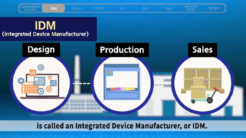
In the semiconductor ecosystem a company that takes charge of the entire process from designing to manufacturing and sales is called an integrated device manufacturer or IDM. Samsung Electronics and Intel are good examples of this.
This model is becoming increasingly difficult to maintain as it requires significant investments in R&D and colossal investments in factories capable of producing very small chips.
Under these conditions, it is hard to be competitive everywhere.
IDMs have a heterogeneous level of integration, meaning they can produce for third parties and/or outsource part of the production to foundries. IDMs with limited production capacity are called "fablight" players. This is the case for companies like STMicroelectronics or Texas Instruments.
Intel and Samsung, on the other hand, are more integrated. Samsung is actually the second-largest chip producer, with approximately 12–15% of global foundry market share as of 2024.
But there are also companies that specializes in Design, Production or Testing.
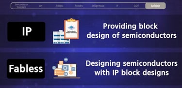
2) Fabless

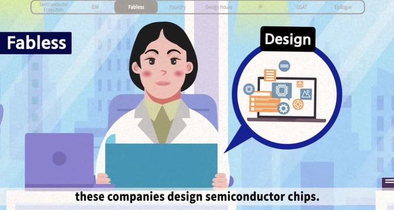

The first category is a fabless company which specializes in Chip design.
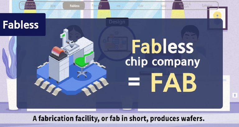

“Fab” or fabrication refers to the semiconductor production line and “less” means the absence of something. In other words, a Fabless is a Semiconductor Company without a production line. which means that it doesn't produce semiconductors. with their knowledge and technology these companies design semiconductor chips. Hence companies that produce a wide range of products but in small amounts and keep technological diversity tend to be fabless companies.
Something to understand before we go into the following point.
The Nanometer Race
You must have heard of 3 nanometer or 2 nanometer ?
These terms are used when we discuss technological competitiveness of semiconductors. As electronic devices become smaller and more complex, chip sizes are required to be reduced on a nanometer scale.
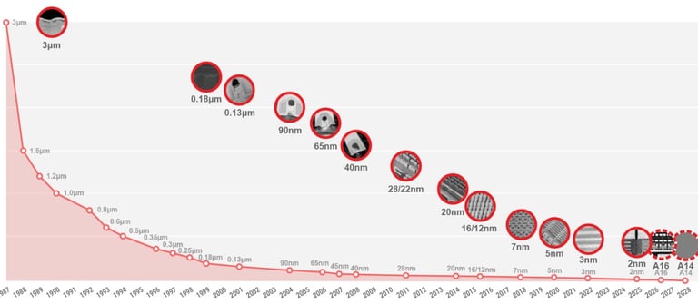
How is this possible ?
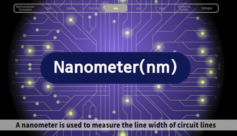
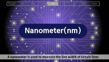
It was possible by reducing the width of circuit lines to increase the number of chips per wafer. A nanometer is used to measure the line width of circuit lines. that's why an ultra-fine process for drawing microscopic circuits onto semiconductor Wafers is important for competitiveness and it leads to Nano competition or ultra fine competition.


EUV technology helps the task of drawing finer circuits onto a wafer, we will talk about that technology later.
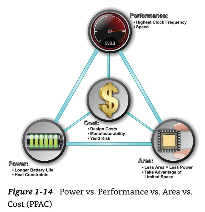
The PPA Triangle: Performance, Power, Area
For semiconductor companies focused on the design, manufacturing, assembly, and integration portions of the value chain, the goal is to achieve the Highest Performance, using the Lowest Power and the Smallest Area possible. These three key design metrics are typically measured in clock frequency (Hz), watts, and nanometers (nm), respectively.
Each semiconductor design may trade off one of these for the others, depending on the application. For example, a team designing a chip for a server in a data center with plenty of space and an industrial grade power source may focus on performance, while not caring as much about size or power. A team designing a chip for a battery-powered cell phone, however, may be concerned more about power and size than performance. For any given application, the goal is to optimize a chip design along these three constraints at the Lowest Cost and in the Shortest Time frame possible.
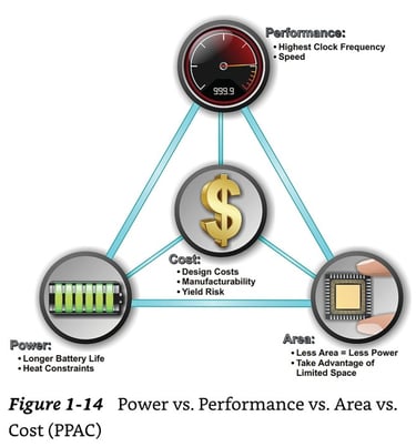
Skyrocketing Design Costs
The cost of designing new chips is skyrocketing due to miniaturization.
5 nm chips are already highly advanced, but since the end of 2022, the industry has been capable of producing 3 nm chips, and 2nm production is expected by 2025–2026.
Cost of designing a new chip in 2020 :

Major companies in this category include Nvidia, AMD, Qualcomm, and Broadcom.
However, some companies outside the semiconductor industry have also entered chip design. Apple, for example, is developing its own chips to control the entire smartphone production value chain.
This is not surprising, as Apple is the world's largest chip consumer, with a spending of $53.6 billion in 2020. And now spending exceeding $68 billion in 2023.
Other tech giants designing their own chips include Google (TPU for AI), Amazon (Graviton for cloud servers, Trainium for AI training), Microsoft (Maia for AI), and Meta (MTIA). This trend of hyperscalers designing custom silicon is accelerating and reshaping the fabless landscape.
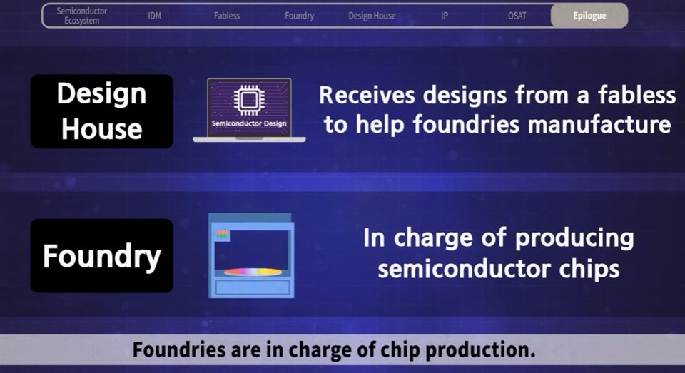
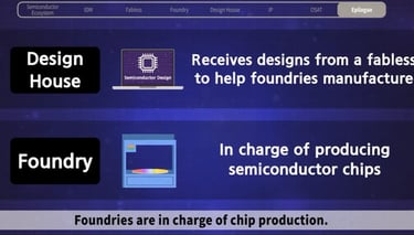
3) Foundry

Companies thar handle only the manufacturing part are called a foundries :
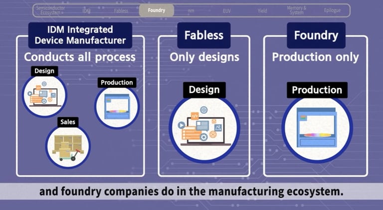
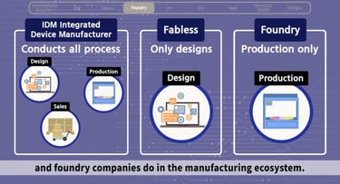
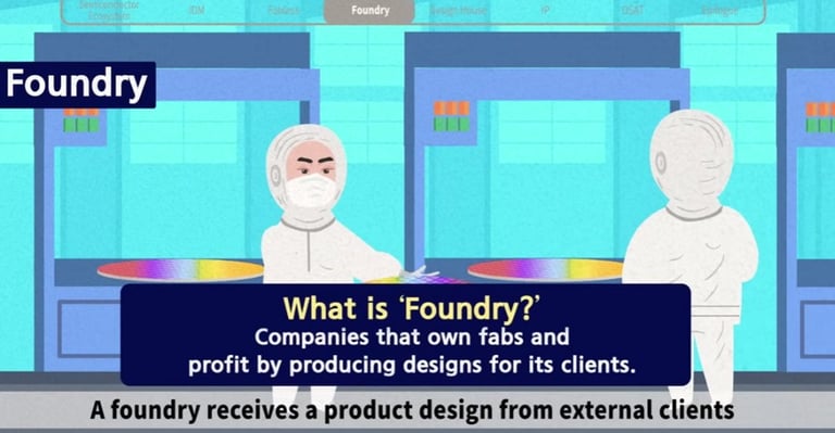
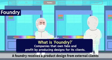
based on designs made by a fabless chip company, they execute the steps of manufacturing we saw before :
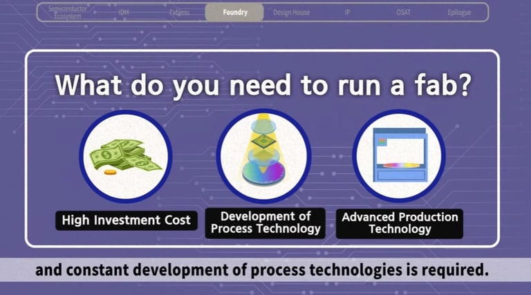
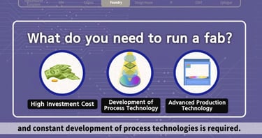
Foundries are companies specialized in manufacturing chips on behalf of their client designers. However, a single semiconductor production line is extremely costly and constant development of process technologies is required. This is why, only a few companies have the capacity to do this.
As such, The same thing as fabless companies applies to semiconductor factories:
As miniaturization accelerates, the investments required to build suitable factories increase. According to Intel, the average cost of a state-of-the-art factory is $15–20 billion for leading-edge fabs (as of 2024).
With very high fixed costs, only a limited number of companies can operate. Therefore, this segment is highly concentrated.
The main players are:
• TSMC: The Taiwanese company is by far the largest, with 60% of the market share in 2024 and 90% for chips smaller than 7 nm.
• UMC: Also a Taiwanese company, it is the second-largest foundry globally with 6.9% of the market share, focused on mature nodes (28nm and above).
• GlobalFoundries: The leading American foundry, representing 5.8% of the market share.
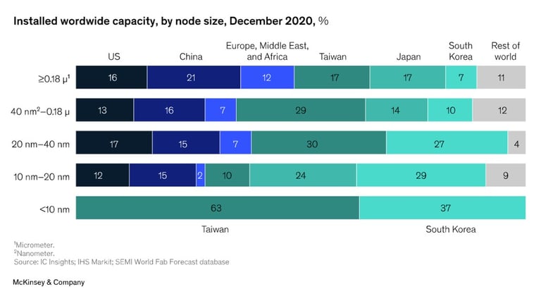
It can be seen that production is heavily concentrated in Taiwan.
To be precise, this is not entirely the case. Europe, the United States, and China together account for 50% of production.
However, the finer the chips, the more the Taiwanese and Asian dominance becomes evident.
It’s simple: 0% of chips smaller than 10 nm were produced outside of Asia in 2020.
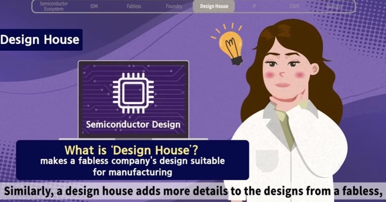
4) Design House

A design house is a bridge that connects a Fabless and a Foundry. It optimizes a fabless company's design so that it is suitable for the production facilities at a Foundry.

A design house is a bridge that connects a Fabless and a Foundry. It optimizes a fabless company's design so that it is suitable for the production facilities at a Foundry.
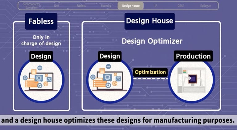

Let's compare it to constructing a building. It starts with an exterior concept design. Based on that, materials used in the building are selected. The details of the interior and exterior design process follow similarly. A design house adds more details to the designs from a fabless so that The Foundry can produce it.
In summary, a fabless only designed semiconductors and a design house optimizes these designs for manufacturing purposes.
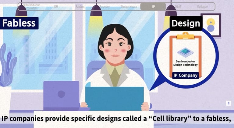
5) IP company

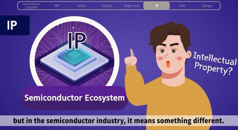

there are also IP companies. Generally, IP means “intellectual property” but in the semiconductor industry it means something different. IP companies provide specific designs called a cell library to a fabless, IDM or Foundry and receive licensing fees or royalties on the IPs (IP cores).

in summary, IP companies only sells its design licenses and does not manufacture products of its own brand.
The dominant IP company is Arm Holdings (UK). Arm’s processor architectures are licensed by virtually every smartphone chip designer (Apple, Qualcomm, Samsung) and increasingly by server and AI chip designers. Arm does not manufacture anything—it purely licenses its designs. Other notable IP companies include Synopsys and Cadence (which also provide IP cores alongside their EDA tools), and Imagination Technologies.
6) OSAT

An Outsourced Semiconductor Assembly and Test company or OSAT, packages and test semiconductors.
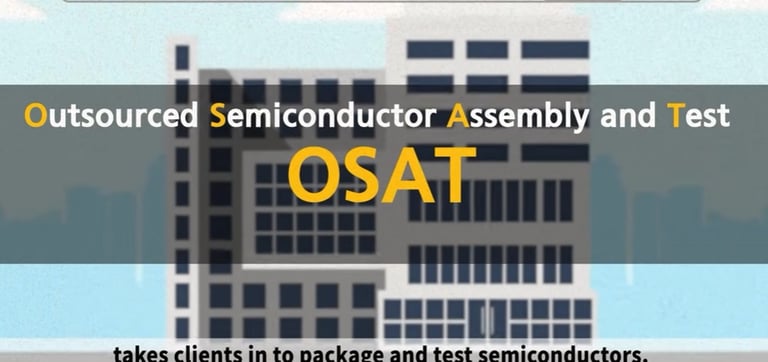

Basically, it takes care of the back-end processes OSATs handle testing and packaging semiconductors from foundries. As it is an essential part in expensive electronic gadgets, High reliability is imperative.
7) EDA Companies
Before any chip is physically made, it must be designed using specialized software, just like architects use CAD software before construction begins. These software tools are called EDA (Electronic Design Automation) tools.
Two companies dominate this market with a near-duopoly:
• Synopsys: The largest EDA company. Their tools are used to design, simulate, and verify chip designs before they go to manufacturing.
• Cadence Design Systems: The second-largest. Together with Synopsys, they control ~70% of the EDA market.
Without these tools, no modern chip, from a simple microcontroller to Nvidia’s most advanced GPU, could be designed.
EDA is an essential but often overlooked part of the semiconductor value chain.
Trend of the Semiconductor industry : Fragmentation
How come the semiconductor industry Become so fragmented ?
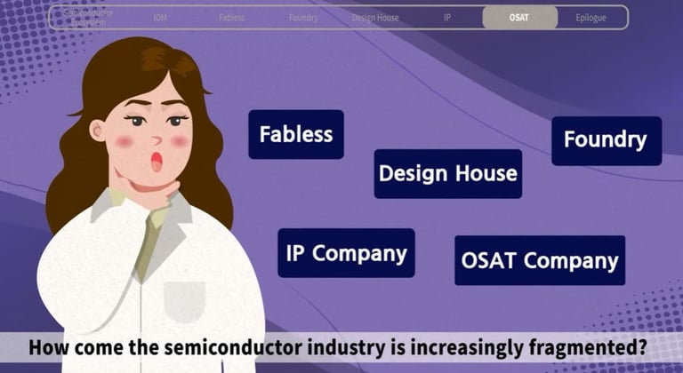
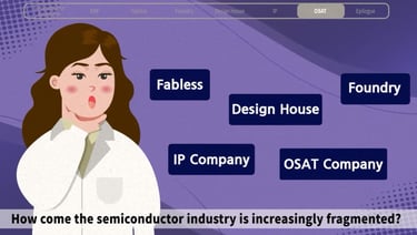
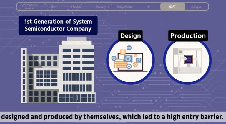
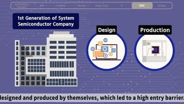
Until the 1980s there were no distinctions between a Fabless and a Foundry, the first generation of system semiconductor companies designed and produced by themselves, which led to a high entry barrier.
When foundries entered the market and took care of Contract manufacturing, it became an opportunity for many fabless companies to emerge in the industry.
In summary :


Equipment Manufacturers
Now, if you have noticed, there are 2 elements of the semiconductor value chain I haven’t talked about : Foundry Equipment, and The suppliers of Raw components.
A good way to look for the companies that dominates those market is to lookthe supplier of a foundry like TSMC: :
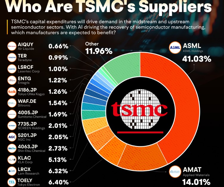

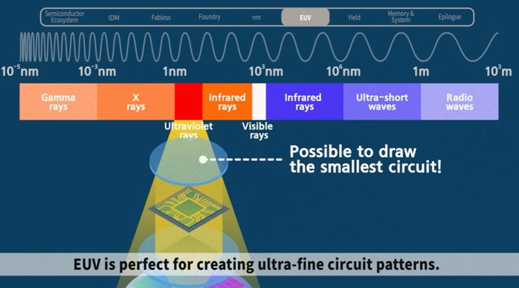
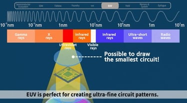
ASML is particularly interesting. They hold 60% of the market share in lithography equipment. They have a de facto monopoly because they are the only ones mastering EUV (Extreme UltraViolet) technology.
What is EUV ?
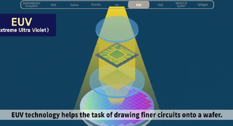
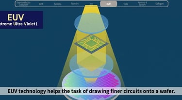
Extreme UltraViolet or EUV is used in a photolithography process to draw circuits onto wafers. Thanks to its short wavelength among all the light sources used in the process EUV is perfect for creating ultra fine circuit patterns we can say that it's equal to switching a blunt pencil to a mechanical pencil to draw.
In 2024–2025, ASML began shipping its next-generation High-NA EUV machines, which use a larger numerical aperture to print even finer details. These machines cost approximately €350 million each and are essential for manufacturing at 2nm and below. Intel was the first customer to receive a High-NA EUV system.
https://www.asml.com/en/products/euv-lithography-systems
KLA Corporation is equally interesting in testing and diagnostics. They are the uncontested leader and hold the lion's share with 50% of the market.
I like Applied Materials and Lam Research a bit less because, though they are more diversified, they don’t have clear competitive advantages that would allow them to completely dominate their segment.
In the link you can find the leader in their field and what they specialize in.
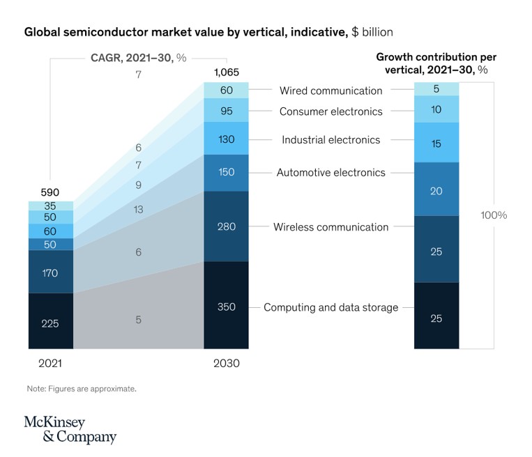
What are the growth prospects for this sector?
The expected growth of this market is 7% per year until 2030, which would value it at over $1,000 billion by that time. This growth will mainly be driven by three sectors that will benefit from major underlying megatrends:
• Data computing and storage: AI and the cloud
• Wireless telecommunications: 5G and the upgrading of smartphones in emerging countries
• Automotive: The fastest-growing segment, driven by the development of autonomous and electric vehicles.
Growth projection between 2021 and 2030 for the semiconductor market - Source: McKinsey

What are the different types of chips?
There are many types of chips. Some are used to store information, others perform simple or complex calculations, and some capture information from the outside world :
1. Digital Chips
These chips perform calculations and store information. They use binary language and process only digital data.
a) Logic Chips
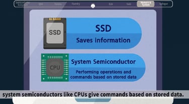
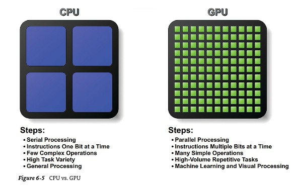
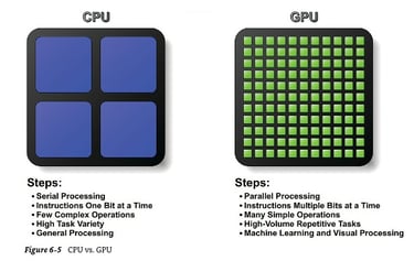
CPU (Central Processing Unit):
These are processors that execute calculations.
Found in all PCs, smartphones, etc.

GPU (Graphics Processing Unit):
Initially designed to optimize graphics processing.
Due to their architecture, they are now the most powerful chips.
Their computing power makes them essential for industries such as cryptocurrency mining and AI.
NPU / AI Accelerator: A newer category of logic chip specifically designed to accelerate neural network computations. Examples include Google’s TPU, Apple’s Neural Engine, and custom ASIC chips designed for AI inference. This category barely existed 5 years ago and is now the fastest-growing logic chip segment.
ASIC stands for Application-Specific Integrated Circuit. As the name implies, ASICs are designed for a specific purpose (Maxfield, 2014). By designing a chip from the ground up, ASICs have several performance advantages including high speed, lower power consumption, smaller area, and lower variable manufacturing costs at high volumes (Maxfield, 2014). The main drawback for ASICs is the significant upfront development costs that go into their design (Cadence PCB Solutions, 2019). Building a chip is a capital and labor-intensive process that requires teams of highly qualified and well-paid engineers. Even if a chip is taped-out (finished) and sent to the fab for manufacturing, there is always the risk that yields are low, or that the ASIC does not function as intended. No amount of verification, validation, and failure analysis can eliminate the risk of serious flaws, and this risk must be considered when deciding whether developing an ASIC makes sense. Another drawback of ASICs is that they are typically so customized for a given application that they can’t be used in another area. For example, audio devices use digital-to-analog converters (DACs) to convert digital voice or music data which is driven as an analog signal to a speaker. The DAC driving the speaker in your phone is customized for the frequency and performance levels needed for audio. That same DAC can’t be used to convert the digital video signals to drive the LCD screen. Each application needs a different chip, which adds to cost and complexity.
b) Memory Chips
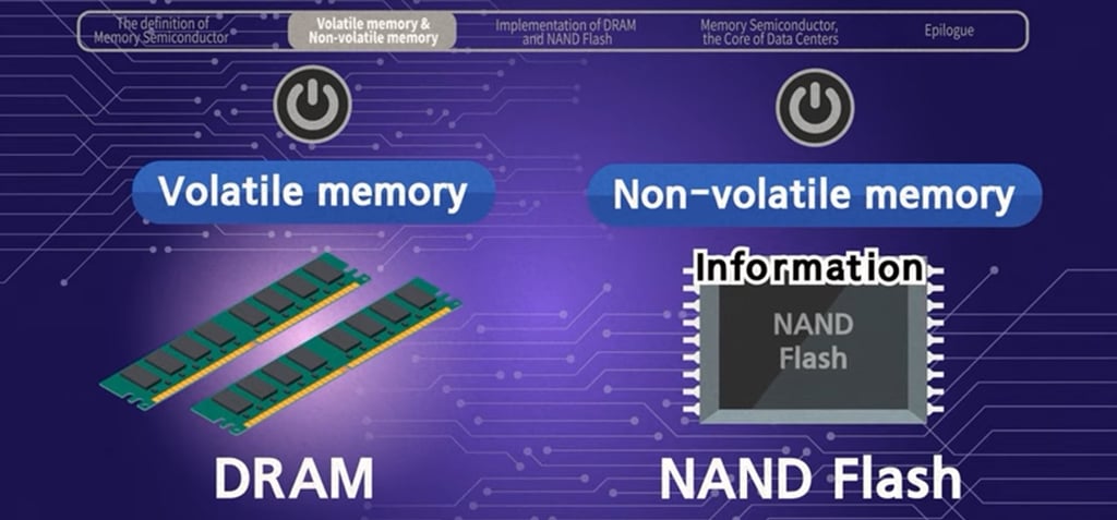
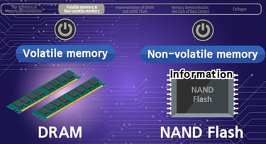
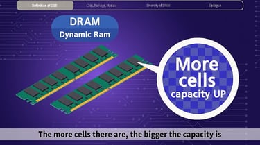
DRAM (Dynamic Random-Access Memory):
Commonly known as "RAM."
Offers a large storage capacity and fast speed but the saved data is deleted once the power is turned off.
What makes DRAM work quickly ?
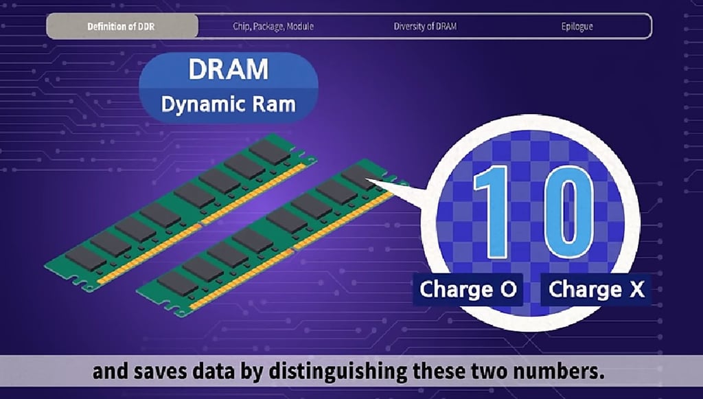
Well, DRAM has cells which are like rooms that save data. The more cells there are the bigger the capacity is.
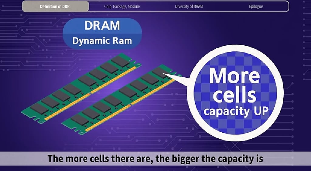
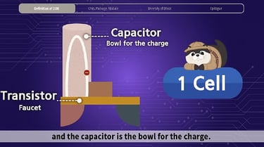
Each memory cell has a transistor and a capacitor, and a capacitor uses zero and one. the basic Digital Data units based on the charges and saves data by distinguishing these two numbers.

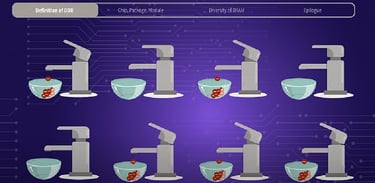
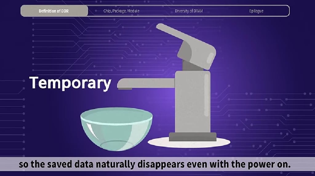
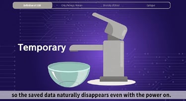
One cell is made of one transistor and one capacitor. The Transistor works like a faucet and the Capacitor is the bowl for the charge.

Out of many bowls, only the faucet for the bowl wanted is turned on to read or save the data.
Thanks to this simple circuit structure, it's fast.

But this bowl stores the charge only temporarily over time the accumulated charge decreases, so the saved data naturally disappears even with the power on.
As a result, Dynamic Ram or DRAM needs a periodical refresh function to manage the data on it.


But once the power is off, it cannot be refreshed, so the stored data is deleted. That's why it is called volatile memory.
Then, is it always beneficial to have many cells per unit area ?
The answer is yes but it also requires High technological skill, we can make the distance between transistors narrower.
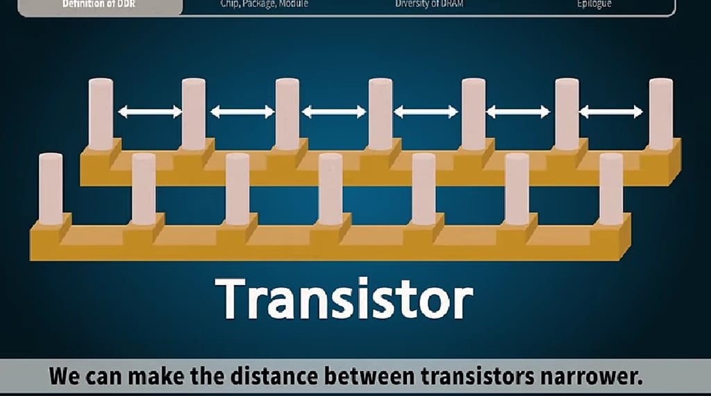
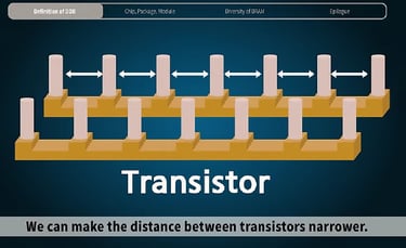
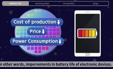
Then chip size can get smaller, which means that we can get more chips from one wafer. In this way, the manufacturing cost goes down, the price gets lower, and power consumption is reduced. In other words, improvements in battery life of electronic devices.
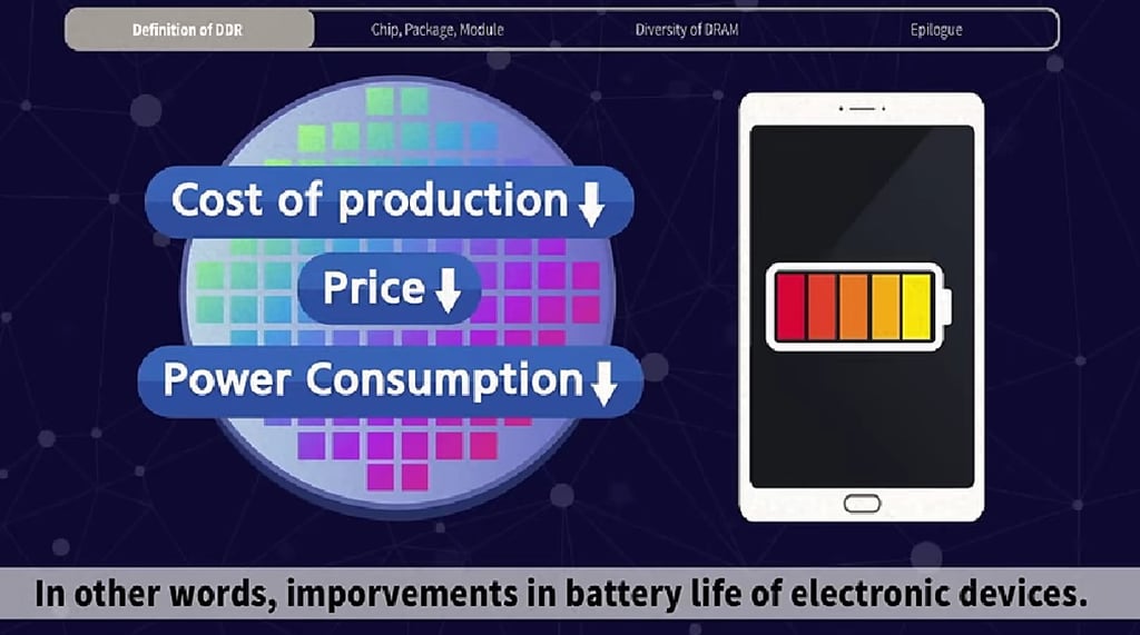
but once the chip size gets smaller, the Capacitor which acts as a bowl for the charge gets smaller too. When the bowl gets smaller and thinner the charge can leak from one cell to another. Even before checking whether it is charged or not, this may cause some kind of Errors. To minimize errors High technological skills are needed.
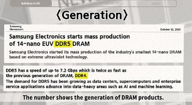
DDR Generations
In the news, we often encounter the terms DDR4 or DDR5? the number shows the generation of DRAM products and with each generation the data processing speed and energy saving capacity are different.

DDR is short for “Double Data Rate”, before we understand what DDR is, let's learn about a CPU's clock rate.
The clock rate measures the frequency of digital signals made of zeros and ones.
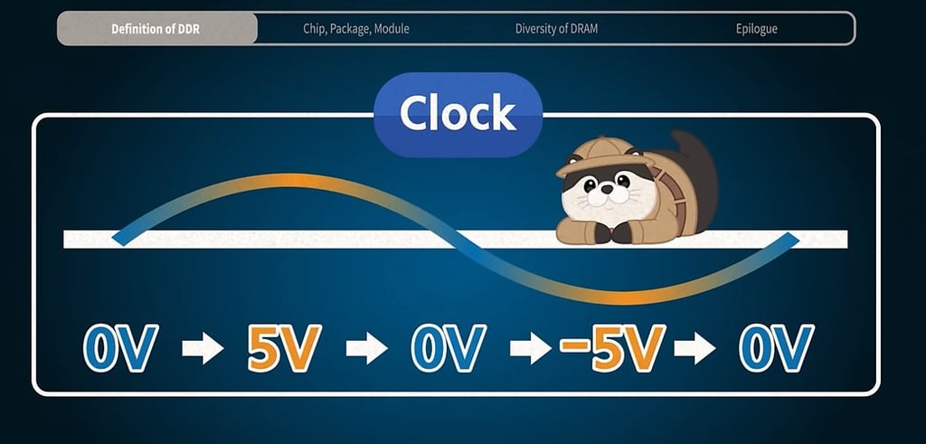
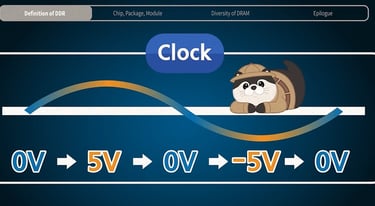
SDR sends signals once per clock cycle, while DDR transfers data twice per clock cycle.
Simply put, one person can complete two jobs in 24 hours instead of one.
Then DDR5 is the fifth generation of DDR, DDR2 achieves speed beyond that of DDR. DDR3, DDR4 and DDR5 represent further improvements in memory technology.
The speed doubles at most with each generation, while the operating voltages decreases, as well as power consumption reduces.
DDR that consumes less power is called low power DDR or LPDDR.
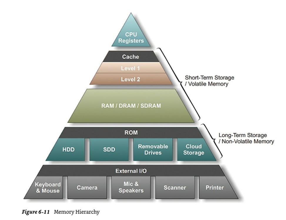
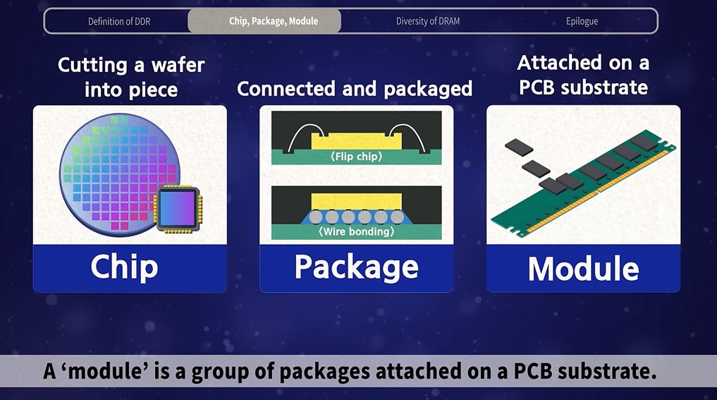
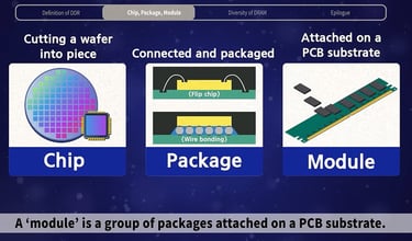
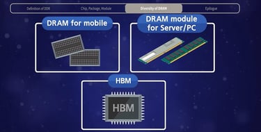
Chip, Package, and Module


First, a chip is what we call a semiconductor which is a small square piece cut from a wafer.
A package means packaged semiconductor chips in a form suitable for the electronic device.
It is destined for a module; a module is a group of packages attached on a PCB substrate.
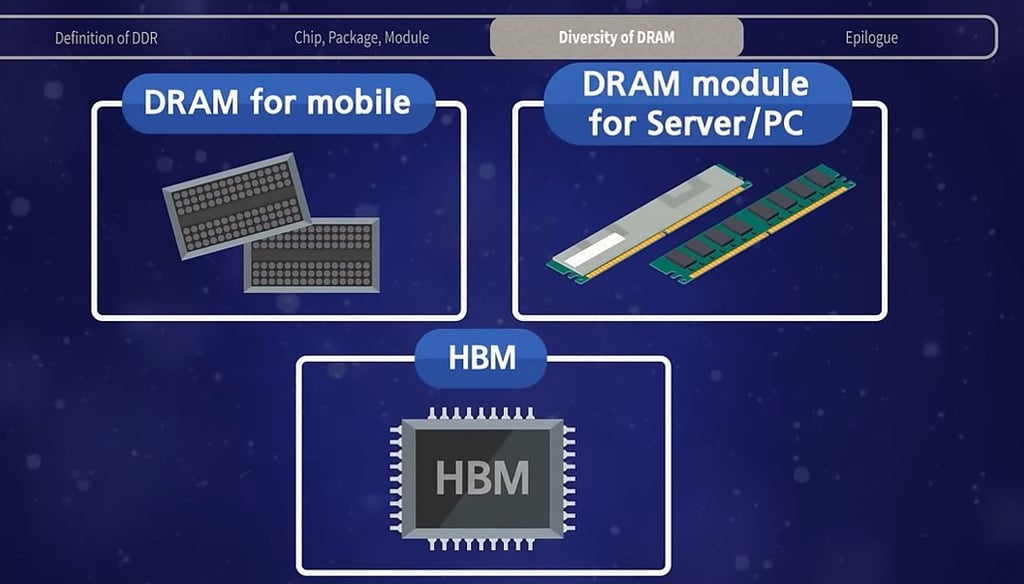
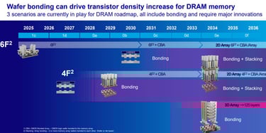
Depending on its purpose there are various types of DRAM:
- mobile DRAM in a package form
- DRAM for servers or PC’s in a module form
- and HBM (high bandwidth memory) for AI.
HBM — The AI Memory Revolution
HBM (High Bandwidth Memory) deserves special attention because it is THE memory technology powering the AI revolution. HBM stacks multiple DRAM dies vertically (currently up to 12 layers in HBM3E) and connects them using TSVs (Through-Silicon Vias), delivering 5–10x the bandwidth of standard DDR memory.
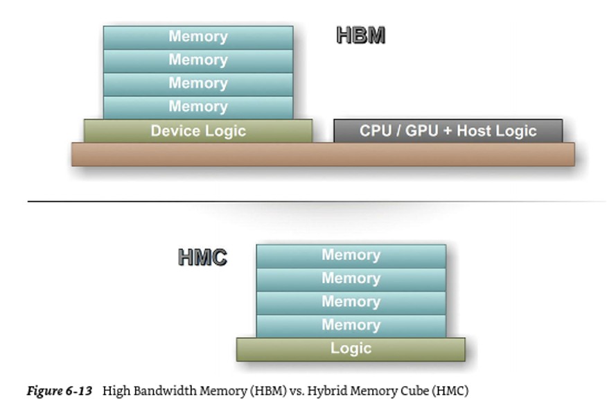
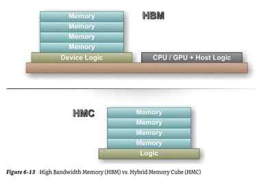
Why does AI need HBM? AI models (like GPT, Gemini, etc.) need to move enormous amounts of data to and from the GPU at extreme speeds. Standard DDR memory simply cannot keep up. HBM solves this by providing a much wider data highway right next to the GPU.

SK Hynix dominates the HBM market (~50%+ share), followed by Samsung and Micron. Demand has exploded: HBM revenue was ~$2B in 2022 and is projected to exceed $25B by 2025. Every Nvidia H100 and H200 GPU contains multiple HBM stacks.
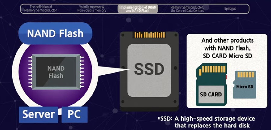
NAND:
Unlike DRAM, these chips store information even when the device is turned off.
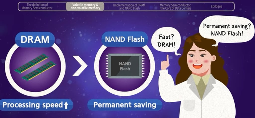
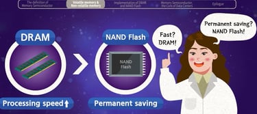
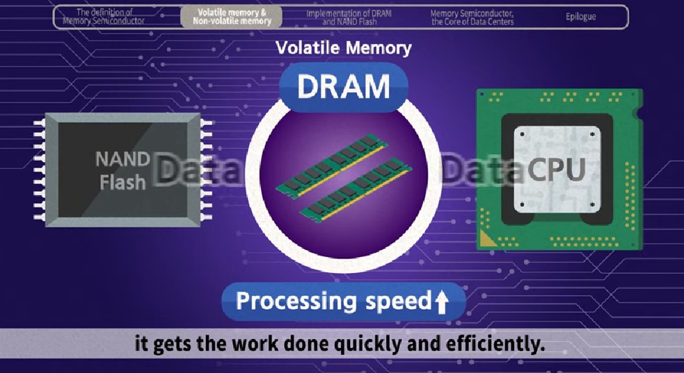
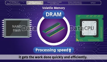
So, we use DRAM where fast processing speed is required and use NAND flash where permanent data saving is required.
Here is an example, you were preparing your dinner you opened the fridge and realized that it's too messy to find what you need. You take out ingredients for cooking and put them on the countertop we can say that the fridge where you put all of the ingredients is NAND flash, and the countertop where you spread the ingredients you need is DRAM.


Without a countertop, it will be really frustrating to cook. It is the same for a computer.
A CPU performs all types of data processing operations. In order to do that, the CPU keeps reading the data saved on the computer. But the problem, is NAND Flash is too slow to catch up with the speed of the CPU, NAND flash is not a perfect partner for the CPU.
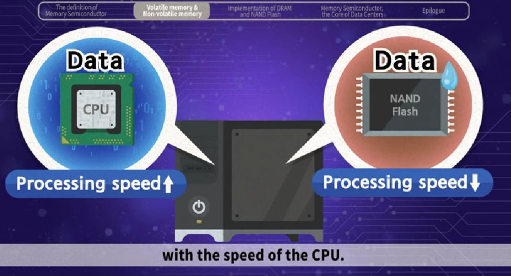
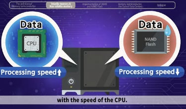
Now, here comes the volatile memory DRAM. DRAM is faster than NAND flash, so it can give and take the data needed by the CPU right away.
That's what DRAM does between the CPU and NAND Flash. It gets the work done quickly and efficiently based on the required purpose and capacity, either DRAM or NAND Flash is chosen to use for PCs, mobiles or servers.
For servers and desktops that require a large capacity, DRAM modules collections of DRAM chips are used to provide what is necessary.
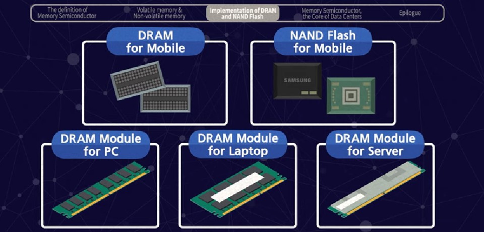
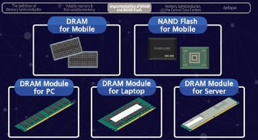
An SSD is largely composed of The NAND Flash, which is used for servers and PCs when it comes to memory semiconductors.
Data Centers and Memory
A data center is important, a data center is a facility that stores and processes all sorts of data we can imagine that enormous amounts of data are stored in a big piece of land the photos and videos we post on our social media channels are saved in this data center or the training of LLMs. In terms of protecting a huge amount of data a server's stability is the most important that is why data centers need fast and stable memories even if they are expensive.


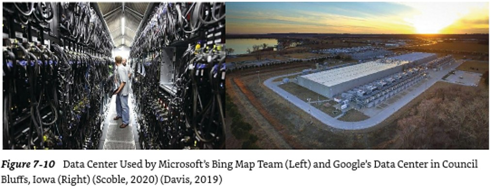

As 5G, IOT and Cloud Computing and AI become a bigger part of our daily lives, memory semiconductor becomes more important. The focus is on how much it can save and how fast it can process. Another important factor is how small the size is and how efficient the power is.
2. Analog Chips
These chips read data from the real world, such as from a thermometer, and convert it into binary language.
Analog chips are less glamorous than GPUs but equally essential. They include power management ICs (PMICs), signal converters (ADC/DAC), sensors, and amplifiers. Every electronic device needs analog chips to interface with the real world. Texas Instruments and Analog Devices are the market leaders. The analog market grows more slowly than digital (~5–6%/year) but is highly profitable and less cyclical.
Value Chain of the Semiconductor Industry
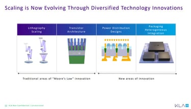
To meet the ever-growing demand for computing power, a real race for miniaturization has begun.
In 1965, Moore, co-founder of Intel, stated the famous law that bears his name. He predicted that the number of transistors in a chip would double every year. In 1975, he revised his prediction to a doubling every two years.
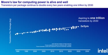
Even today, this law is still more or less respected.
This technological race is driving up design and production costs, forcing industry players to specialize in order to be best equipped to face these challenges.
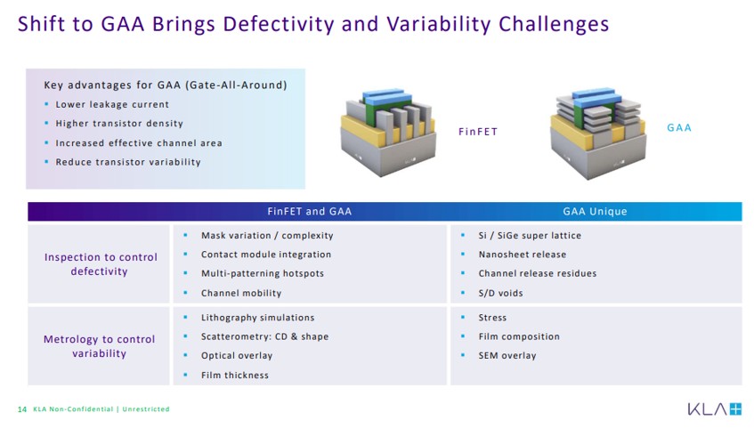
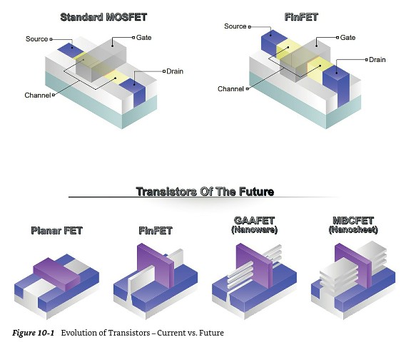
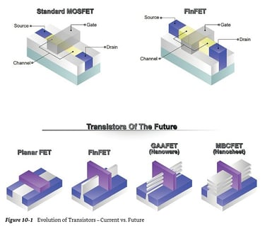
However, many experts argue that Moore’s Law is slowing down. The physical limits of silicon are being approached. This is why the industry is pivoting to advanced packaging (chiplets, 3D stacking) and new transistor architectures (Gate-All-Around / GAA transistors, replacing FinFET) to continue improving performance without solely relying on smaller transistors.
What are the risks for this industry?
A global geopolitical battle
Semiconductors are at the heart of a global geopolitical battle due to their critical importance for sectors such as defense and new technologies.
The United States is doing everything it can to prevent its rival, China, from catching up in this field. And for good reason: even though China has made significant technological progress, semiconductors remain its main import.
Without modern semiconductors, there is no advanced technology.
Thus, the US administration has banned Nvidia and AMD from exporting some of their most advanced GPUs to China and Russia.
That's not all—The US has also lobbied for the Dutch and Japanese governments to prevent their companies from exporting advanced equipment to China (ASML for the Netherlands, Tokyo Electron and Nikon for Japan).
These export restrictions have been progressively tightened through 2023–2025. The October 2022, October 2023, and December 2024 rounds of restrictions increasingly limited China’s access to advanced chips, AI training hardware, and semiconductor manufacturing equipment. China has responded by investing heavily in domestic alternatives (e.g., SMIC, Huawei’s HiSilicon), but remains significantly behind at leading-edge nodes.
Increased dependence on Taiwan
As mentioned earlier, Taiwan is home to a large portion of the manufacturing of advanced chips. This represents a real risk.
For context, Taiwan has been claimed by China since 1949. Several times, they have threatened to invade the island. If this were to happen, the consequences would be immeasurable.
Europe and the United States have fully understood this vulnerability. They have therefore launched ambitious plans to attract investments in this sector.
The United States passed the Chips and Science Act in 2022, which allocates $280 billion in support, including $52 billion in subsidies.
TSMC’s first Arizona fab began production in 2025, with a second fab under construction for advanced nodes. Intel is building massive new fabs in Ohio and Arizona under its IDM 2.0 strategy. Samsung is building a $17B fab in Taylor, Texas. Total announced investments in the US alone exceed $200 billion.
The EU responded quickly with the Chips Act in 2023. It aims to mobilize €43 billion to help Europe achieve 20% of the global market share, which would double its production capacity.
Major EU investments include Intel’s planned €30B fab in Magdeburg, Germany, and TSMC’s joint venture fab in Dresden. However, progress has been slower than in the US, and the 20% target is widely considered ambitious.
Cyclicality of the sector
This industry is cyclical. Texas Instruments created this chart that clearly illustrates this.
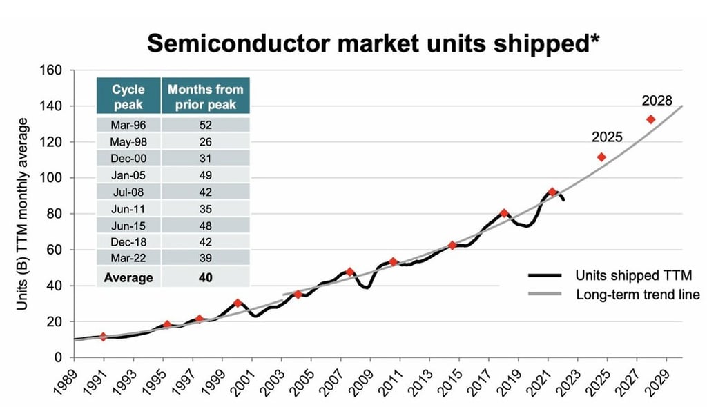
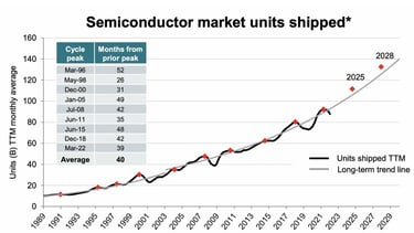
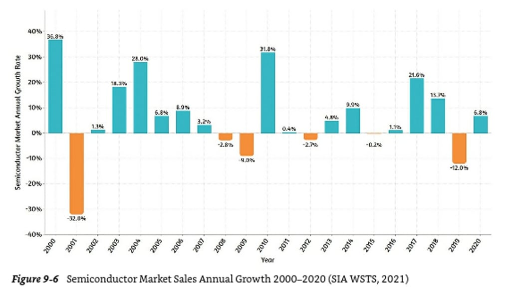
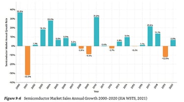
For some companies those cycles can make the difference between profits and no profits so you have to be careful of where in the cycle you are.
Personal Investment Notes
Note: This section contains personal investment opinions and analysis. It is separate from the educational content above. This is not financial advice.
Equipment Manufacturers
ASML is particularly interesting. They hold 60% of the market share in lithography equipment. They have a de facto monopoly because they are the only ones mastering EUV (Extreme UltraViolet) technology.
KLA Corporation is equally interesting in testing and diagnostics. They are the uncontested leader and hold the lion's share with 50% of the market.
I like Applied Materials and Lam Research less because they don’t have clear competitive advantages that would allow them to dominate their segment.
Designers
Nvidia and AMD are particularly attractive. They share the GPU market. However, they are often excessively expensive. And they are far too expensive right now for me with no margin of error for the future they have to beat expectations and beat them impressively, not for me, too much risk of it going a bit less well than expected.
Broadcom has a unique positioning. Specialized in chips for the telecommunications sector, the company is increasingly diversifying into software (especially with the completed acquisition of VMWare). But also expensive although less than Nvidia and AMD.
Foundries
Although TSMC is in a near-monopoly situation, the geopolitical risk is far too significant in my view.
Source:
https://www.micron.com/educatorhub?SelectedValues=%2Fk12-stem%2Fartificial-intelligence
https://semiconductor.samsung.com/support/tools-resources/fabrication-process/
https://www.asml.com/en/investors/investor-days/2024
https://newsroom.lamresearch.com/newsroom
https://www.mckinsey.com/industries/semiconductors/our-insights/the-se...
https://www.samsung.com/semiconductor/newsroom/
https://quartr.com/insights/company-research/understanding-the-semicon...
https://www.semiconductors.org/resources/
https://news.skhynix.com/semiconductor-101-roundup-sk-hynix-quick-guid...
https://setr.stanford.edu/technology/semiconductors/2025
https://www.youtube.com/@Asianometry
https://www.asml.com/en/technology/lithography-principles/what-is-euv-...
© 2025-2026. All rights reserved.
Centro Research
info@centroresearch.eu
Investment research of securities and markets
Reports and other shared materials should not constitute as financial advice. Investment decisions require individual due diligence and one should seek qualified counsel.