ASML Stock Analysis
Analysis into ASML company and stock as a potential investment.
STOCKSEMICONDUCTORIN-DEPTH ANALYSIS
Rafael CARRARA
2/8/202678 min read
November 2024
- ROE = 47% > 10%
- P/E = 35.3 < 22.5 X
- revenue growth over the last 5 years
-profit growth over the last 5 years
-shares outstanding increased less than 5% over 5-years
-5 year cash flow growth
-5 year price to free cash flow = 95.61 < 22.5 X
-They have more cash than debt
Business Overview
ASML is a leading supplier to the semiconductor industry. The company provides chipmakers with hardware, software and services to mass produce the patterns of integrated circuits (microchips).
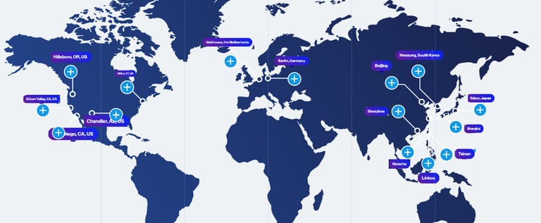
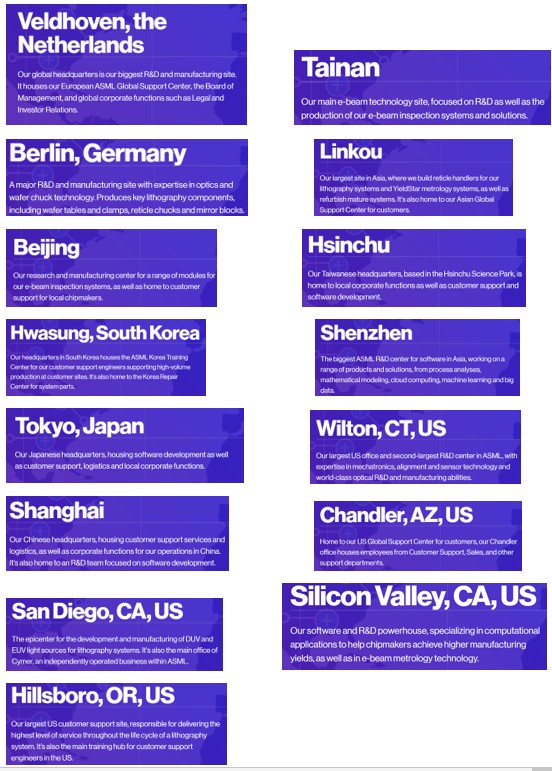
ASML is a multinational company headquartered in Veldhoven, the Netherlands, with offices across EMEA, the US and Asia. Every day, ASML’s more than 43,000 employees (FTE) challenge the status quo and push technology to new limits. ASML is traded on Euronext Amsterdam and NASDAQ under the symbol ASML.

Their Vision and strategy
“Our vision is that we enable ground-breaking technology to solve some of humanity’s toughest challenges. And, our strategy and priorities are designed to deliver on these points and create long-term sustainable value for our stakeholders.”
News in 2024 :
2023 Results

2024 Results

ASML, the Dutch company, is probably one of the best European stock right now. However, after a stellar performance since its IPO in 1995, the stock has lost more than 30% from its highs in July 2024.
Although the quality of this company is recognized by many investors, this stock remains very complex because of valuation and the growth expectations that are included in the price.
Before diving into ASML’s history, it is essential to understand what ASML does. To do so, one must grasp the semiconductor industry’s value chain.
In summary, producing chips requires a complex process that is divided into several stages, as outlined in the simplified diagram below.
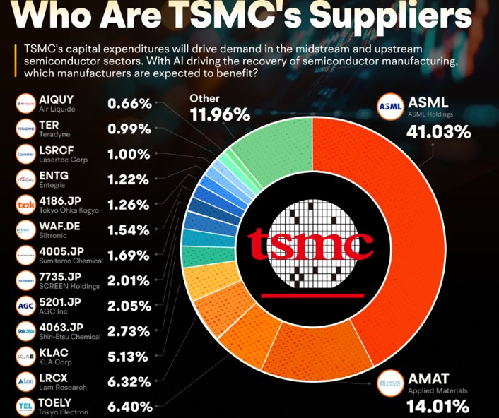

ASML Equipments account for most of TSMC’s capital expenditure.
The lithography machine is the most important piece of equipment in any chip factory, and without doubt the biggest investment in a facility that can set you back 15 billion dollars to build. It is easy to see why working at ASML is known to come with a little pressure.
For many, the semiconductor industry may seem abstract. So let’s start by explaining the principle of lithography.
ASML focuses on the key step of photolithography (or lithography). Why is this so important? Because this step generates the most added value, serving as the main driver of chip miniaturization and enabling Moore’s Law to hold for decades.
We can see that when we look at TSMC List of suppliers :
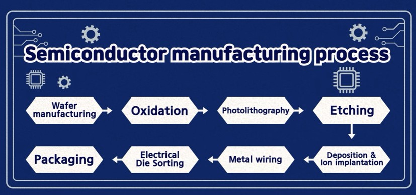
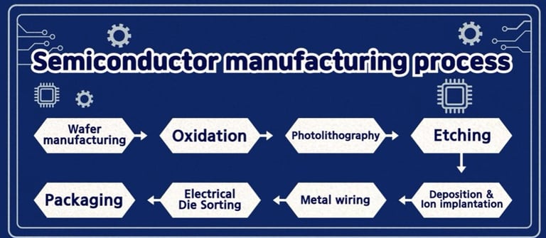
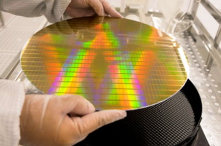
To produce chips, integrated circuits must first be drawn and then etched onto a silicon wafer.
Photolithography process :
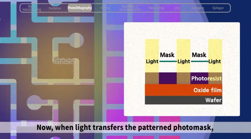
Just as you draw blueprints to build a building, you draw a circuit design onto a wafer, which is called the photolithography process.
It is called photo for short, because it is similar to developing a photo taken on a film camera. With semiconductors, a photo mask functions as the film. A photo mask is a glass substrate with a computer designed circuit pattern.
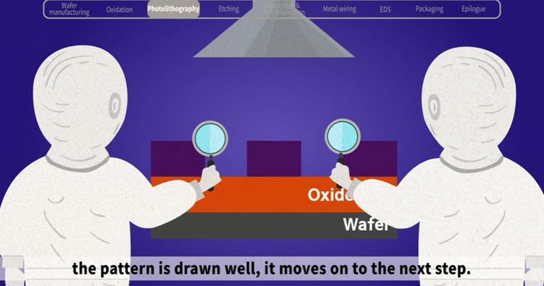
In order to draw the circuit on the wafer, the photoresist, a material that responds to light is applied thinly and evenly on the oxide film previously placed on the wafer :
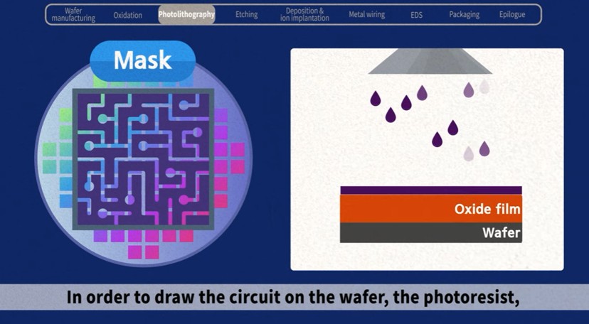
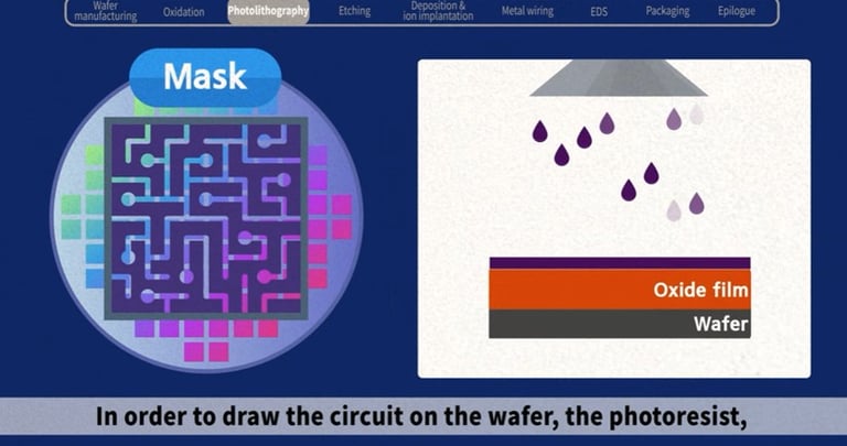
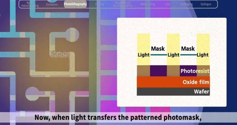
Now, when light transfers the pattern photo mask the circuit is drawn on the wafer surface, just like developing a photo.
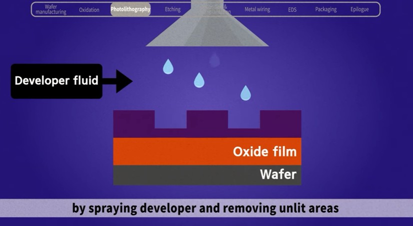
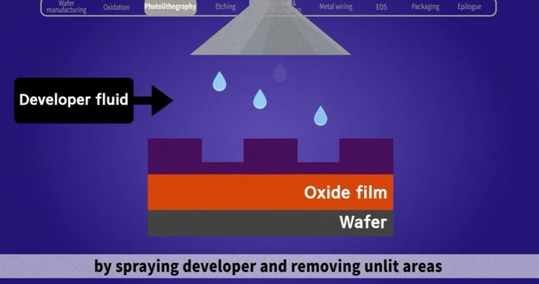
A circuit pattern is imprinted on the wafer by a developer fluid and removing unlit areas from the areas that are exposed to light.
After an inspection of the wafer to check whether the pattern is drawn well, it moves on to the next step.

Now that we’ve covered the basics of lithography, we can move on to what really interests us—ASML and how they became indispensable.
The Story of ASML :
ASML was founded in 1984 as a joint venture between two Dutch companies: Philips and ASM International (a publicly traded company).
In fact, ASML stands for “ASM Lithography.”
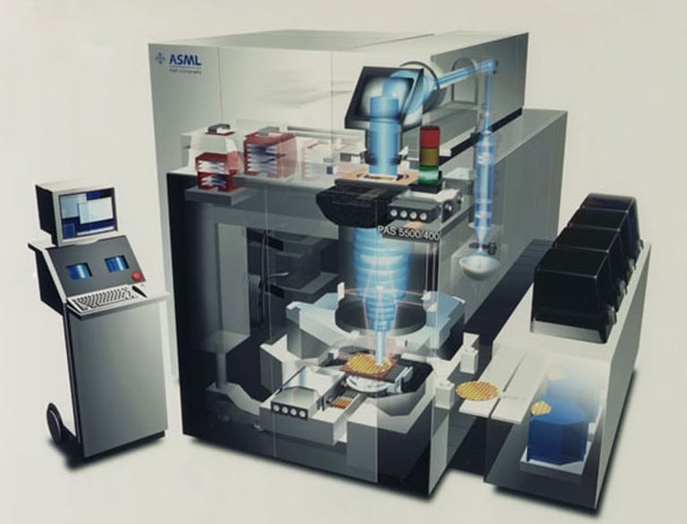
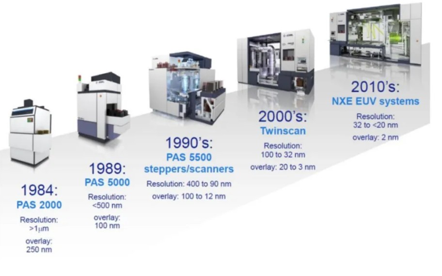
The first machine, the PAS 2000 stepper, was launched in 1985 :
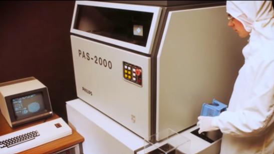
In its early years, ASML struggled to compete in this high-tech industry. For its first six years, the company was unprofitable, leading ASM International to sell its shares to Philips and several banks.
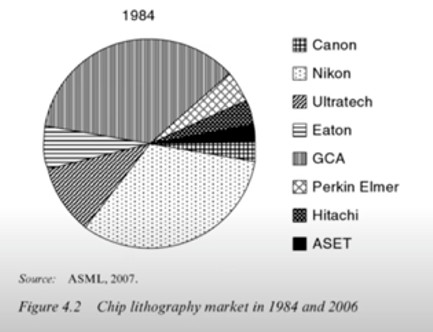
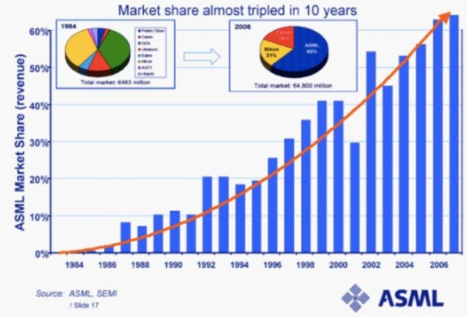
In 1984, the market was dominated by American companies such as Ultratech, Eaton, GCA, and Perkin Elmer.
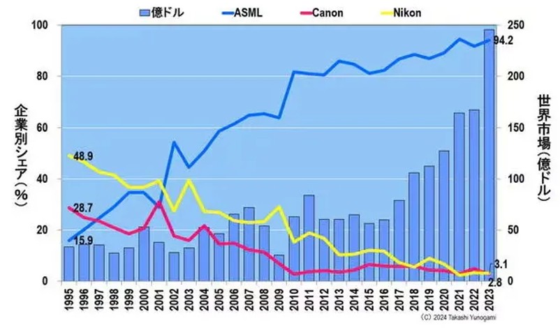
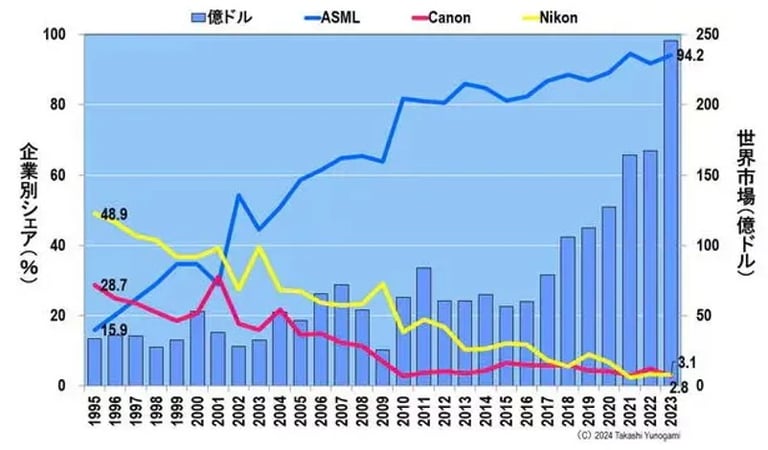
However, these firms began losing ground, while Japanese companies Nikon and Canon rapidly gained market share, becoming dominant by the late 1980s.
Meanwhile, ASML still struggled to establish itself in this highly competitive industry :
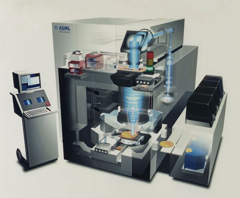
In 1990, Philips decided to part ways with ASML, no longer willing to support a loss-making company. Despite this setback, ASML continued to fight for survival and, in 1991, launched its first commercial success: the I-Line stepper, the PAS 5500.
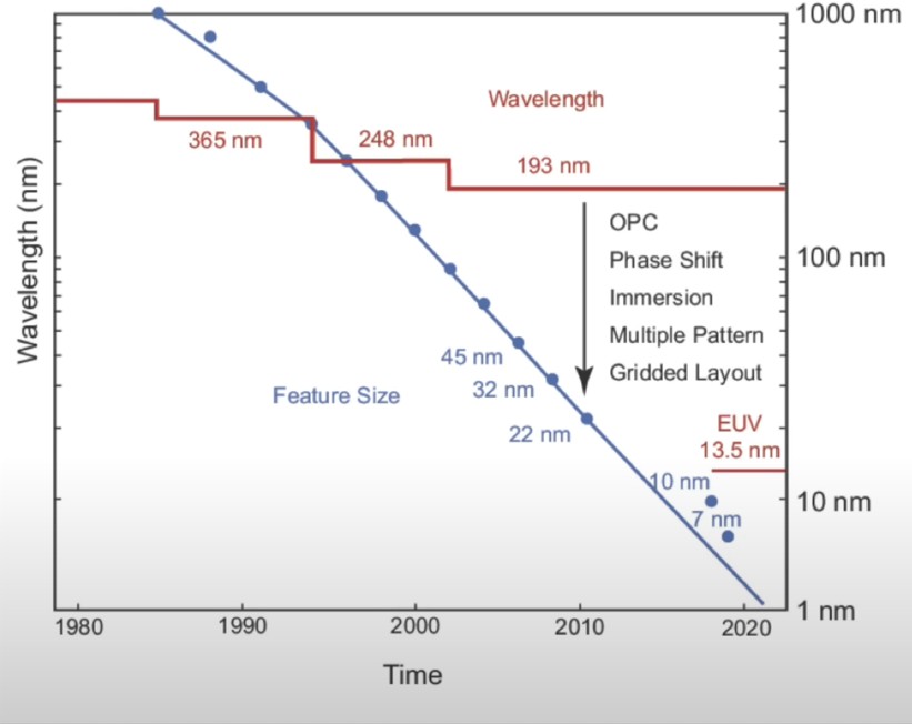
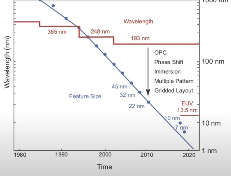
The I-Line technology used light with a wavelength of 365 nm, a major technological breakthrough at the time. This advancement allowed chipmakers to design smaller structures, enabling the production of more advanced chips.
During the 1980s and 1990s, advances in lithography transformed the industry. It became easier to reduce transistor size by decreasing the wavelength of light.
This approach proved so effective that it outperformed all other alternatives for improving miniaturization and increasing the number of transistors per chip.
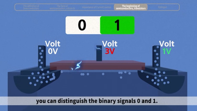
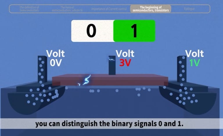
A transistor is a fundamental electronic component used to control the flow of electrical current in circuits. It acts as a switch or amplifier for electrical signals.
Moore’s Law is an observation made in 1965 by Gordon Moore, co-founder of Intel. It states that the number of transistors in an integrated circuit (electronic chip) doubles approximately every two years, allowing for exponential increases in computing power and/or reductions in chip size (which ultimately enabled the production of smartphones).
The success of this product allowed ASML to quickly gain market share in the photolithography equipment sector.
In 1995, ASML capitalized on this breakthrough and the consolidation of the lithography machine market to continue its development, which required significant capital.
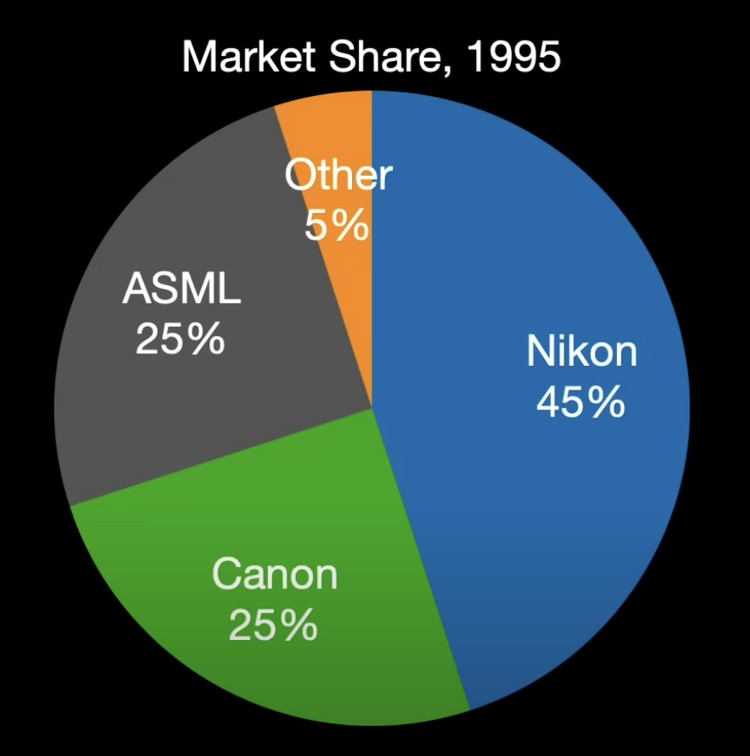

By the mid-1990s, an oligopoly formed between Canon, Nikon, and ASML, with other players either leaving the market or being absorbed.
Three major technological advancements, which ASML mastered, would then allow the Dutch company to become the uncontested leader in lithography in the 2000s.
How ASML Became the Uncontested (and Unquestionable) Leader in Lithography Before EUV
I generally don’t go that deep into the history of a company usually BUT I genuinely believe it’s crucial for understanding the dynamics of this market and the competitive advantages that allowed ASML to achieve its unparalleled dominant position.
Breakthrough 1: The TWINSCAN
With the arrival of the new millennium, ASML understood that it needed to adopt a radically innovative approach to provide its customers with a real productivity boost.
It wasn’t just about further reducing the minimum resolution. ASML and its competitors aimed not only to enable the production of increasingly advanced chips but also to do so in an economically viable way.
Three parameters had to be optimized simultaneously:
• Resolution: Measured by the minimum resolution size, in nanometers.
• Productivity: Calculated by the number of wafers processed per hour.
• Yield: Evaluated by various indicators, such as the percentage of dies passing diagnostic tests.
So, even if ASML managed to produce an ultra-high-performance machine that reduced the minimum resolution, it would never be profitable for foundries if it was too slow.

Similarly, if the machine lacks precision or generates too many defects, it reduces the yield and makes the process unprofitable. With a manufacturing process that includes between 800 and 1,200 steps for chips with a 16 nm minimum resolution, it’s crucial for the yield of each step to be nearly perfect for the entire process to be economically viable.
To give a sense of scale, TSMC achieved a yield of 95-96% for 16 nm chips, an exceptional level. It’s hard to grasp the level of engineering required to reach these yields on infinitesimally small components.
Now, let’s get back to TWINSCAN. In the early 2000s, ASML decided to focus its efforts on drastically improving productivity.
As often happens, the idea seems obvious in hindsight, but at the time, it wasn’t. In the 1990s machines, wafers had to be scanned precisely before the pattern was exposed onto them, an essential step that still exists today.
However, back then, scanning and exposure were done separately. Industry players were focused on optimizing productivity by reducing the time for each step independently.
ASML’s idea was different and quite innovative: to save even more time, why not scan a wafer while the previous one is still being exposed?
That’s how the TWINSCAN platform was born.
I also found a more detailed explaination about it in FOCUS : The ASML way :
« The first immersion-machine hit the market in 2004, immediately putting the Japanese competition at a disadvantage. The already expanding Dutch market share was pushed ahead even more by the introduction of another groundbreaking invention: the TwinScan. This new machine could measure for alignment and illuminate at the same time, performing a high degree of complex multitasking that shaved off invaluable time for chip factories. This is how it works: before a new pattern can be printed on a silicone layer, the wafer must first be measured. This information is needed to align it before exposing it, so the new layer will fall exactly on the previous pattern. Already difficult, but the real problems stem from the degree of heat the wafer has to endure in the ovens. This can cause the wafer to warp, like a Pringle potato chip. What looks like a perfectly flat disc to the naked eye is revealed by a microscope to be more like a rugged mountainscape. So, before any measurement can take place, the wafer is carefully suctioned into place, which removes the worst of the bumps. Sensors then record the remaining deviations, creating a detailed 3D map of the surface with all its peaks and troughs. The lithography machine then uses this map to adjust the focal plane during exposure, compensating for the deviations so the chip patterns are projected at an equal sharpness over the whole surface. Think of it like the autofocus on a camera, rapidly correcting the image at miniscule distances and depths. »
The TWINSCAN was the first—and remains to this day the only—lithography system capable of scanning and exposing wafers simultaneously. While the wafer on table one is being exposed, another wafer is loaded, aligned, and mapped on table two.
The productivity gain is enormous. With the launch of its first model, the TWINSCAN AT:750T, ASML achieved immediate commercial success.
As a result, ASML’s market share nearly doubled in just one year, going from just under 30% in 2001 to over 50% in 2002.

Breakthrough 2: Immersion Lithography
Before mastering Extreme Ultra-Violet (EUV) technology, which ASML is the only company to control, ASML had already outpaced its competitors with another revolutionary technology: immersion lithography.
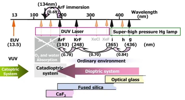
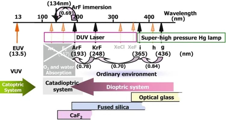
At the turn of the century, the best available lithography used an argon fluoride (ArF) laser light source with a wavelength of 193 nm.
We are already in a system called DUV (Deep Ultra-Violet).
These machines could etch nodes with a minimum size of 90 nanometers. Successive improvements in this technology allowed the industry to move to 65 nanometer nodes.
In theory, the transition was supposed to be smooth, moving from 193 nm light etching to 13.5 nm light with the arrival of EUV.
However, an unexpected development changed the situation: EUV was delayed by 10 years.
While waiting for this advancement, the industry had to push DUV lithography systems to their limits. One of the key techniques for this was immersion lithography, where the 193 nm light is projected through water to improve resolution.
How Does Immersion Lithography Work?
Now, let’s move on to the less pleasant part of this newsletter—the technical section.
In the field of lithography, their reference equation isn’t one of supply and demand, but Rayleigh’s formula:
CD = k1 × λ / NA
Where:
• CD stands for “Critical Dimension,” or the minimum resolution that is being optimized by reducing it as much as possible.
• k1 is a factor with a physical limit that we’ve nearly reached and can no longer optimize.
• λ represents the wavelength of the light.
• NA is the numerical aperture of the optics, which defines the amount of light that can be captured.

To reduce the minimum resolution, there are two parameters that industry players can adjust: the wavelength and/or the numerical aperture.
When aiming for EUV, the goal is clear: drastically reduce the wavelength to make a significant leap forward.
In the meantime, with immersion lithography, by passing the laser through water before it reaches the wafer, the numerical aperture can be increased from a maximum of 0.93 to 1.35 (or even higher).
Small note :
The idea of using immersion lithography wasn’t obvious. For a while, the industry focused on developing a 157 nm wavelength light source.
However, in 2002, the project was abandoned because the technical challenges of moving to 157 nm were too significant.
Increasing the numerical aperture, on the other hand, created its own challenges, but in hindsight, they were easier to overcome.
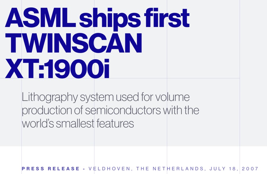
In 2003, ASML delivered its first immersion lithography system prototype to clients: the TWINSCAN XT:1150i.
The first stepper ready for mass production, the XT:1700i, was launched in 2006.
ASML’s Japanese rivals, Canon and Nikon, took longer to develop their own immersion tools.
• Nikon completed its prototype in October 2004, nearly two years after ASML.
• Canon never commercialized theirs, which meant they quickly disappeared from the market starting in the second half of the 2000s.
The race didn’t stop there. After the first generation of immersion machines, ASML and Nikon continued developing the next generations.
These more advanced systems reached a numerical aperture (NA) of up to 1.92, enabling foundries to achieve a minimum resolution of 40 nanometers. However, each advancement brought new challenges, particularly with the immersion liquid and optical systems.
Once again, ASML dominated this race, further solidifying its market leadership. In 2007, they launched their first mass production system, the XT:1900, which would serve as the foundation for all subsequent generations.
Finally, six years later, in 2013, ASML delivered its first system based on EUV technology, after years of delays and billions of euros invested in R&D.
How EUV Became ASML’s Exclusive Domain ?
Of course, ASML wasn’t the only player trying to find solutions to continue adhering to Moore’s Law. To understand the evolution of this groundbreaking technology, we need to go back to 1997.
That year, ASML and the entire semiconductor industry began to consider next-generation lithography. It’s important to note that, in this industry, every technological advancement must happen through consensus.
Why?
Because the capital needed to fund R&D (and the many failures along the way) can only be recouped if all foundries and the entire ecosystem agree to the new standard.
If ASML developed EUV on its own without the other steps in the process being adapted, it would be pointless. This principle applies to other areas too. For example, the size of wafers is the result of a consensus: today, they are 300 mm in diameter. They were supposed to increase to 450 mm, but TSMC chose not to follow, preventing this transition, which could have greatly improved productivity.

The Competing Technologies
In 1997, several potential paths were being considered as successors to 193 nm optical lithography. Here are the main technologies being considered :
X-ray Lithography
Electron Beam Lithography (E-beam)
Extreme Ultraviolet (EUV) Lithography
Each of these options had its advantages and drawbacks, and importantly, its own sponsors.
X-ray Lithography: IBM had invested $1 billion in this technology, which was probably the least costly to operate. However, technical difficulties, particularly with the mask, quickly disqualified it.
Electron Beam Lithography: Bell Labs (later acquired by Alcatel-Lucent, then by Nokia) and Nikon were pushing for the adoption of electron beam lithography.
Extreme Ultraviolet (EUV) Lithography: Intel, already invested in this technology, supported EUV. This technology was the closest to DUV lithography and seemed like the logical next step.
On ASML’s side, the company decided to play all fields by working on both EUV and electron beam projection technologies. For a few years, the two projects coexisted. However, after a few months, ASML pulled out of the electron beam project, as the technical challenges seemed too complex.
Moreover, electron beam lithography had a major flaw: its productivity was too low. Estimates predicted a productivity of only 4.8 wafers per hour, compared to an estimated 42 wafers per hour for EUV.
How ASML Won the EUV Race
ASML focused all its efforts on developing EUV, while Nikon bet on electron beam projection and the development of a 157 nm wavelength DUV system. To strengthen its position, ASML negotiated and obtained a license from the American consortium EUV LLC.
This consortium, founded by key American semiconductor players like Micron and Intel, in collaboration with the U.S. Department of Energy, funded research and filed patents related to EUV technology.
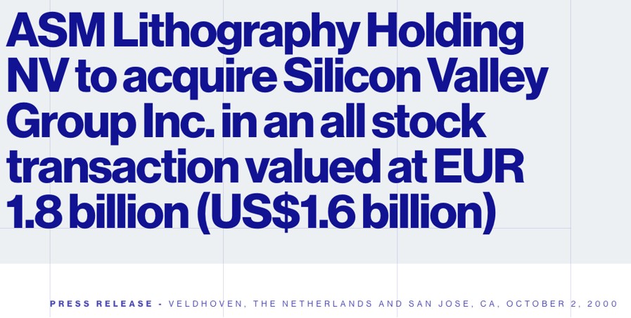
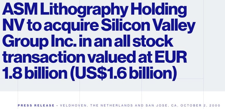
To further accelerate its development, ASML acquired Silicon Valley Group (SVG) in 2000. This relatively obscure American lithography company was also part of the EUV LLC consortium. By acquiring SVG, ASML gained additional technological expertise and intellectual property that gave it a significant edge over its competitors.
This strategic acquisition, along with ASML’s unwavering focus on EUV, allowed the company to dominate the EUV race and secure its position as the undisputed leader in advanced semiconductor lithography.
these events allowed ASML to gain a decisive advantage over its Japanese competitors. More importantly, EUV LLC never granted licenses to Nikon or Canon. As a result, both companies eventually abandoned the development of EUV. ==> MOAT
Canon halted its efforts in 2007 due to financial reasons.
Nikon, on the other hand, persisted in investing in now-obsolete technologies.
ASML took a significant risk at a critical juncture. Above all, they made the right strategic decisions at the right time. In 2006, the first prototype of the EUV system was developed.
By 2013, ASML delivered its first EUV system: the TWINSCAN NXE:3300, marking the culmination of years of research and development and solidifying ASML’s position as the undisputed leader in advanced semiconductor lithography.

However, much more work was required to make EUV both technically and industrially viable.
To further align the interests of its stakeholders and ensure that all the investments were not wasted, while also securing additional funds to continue improving and finalizing the EUV technology, ASML made a radical decision in 2012: it proposed that its major customers participate in funding ASML’s R&D in exchange for shares in the Dutch company.
Intel took a 15% stake in ASML.
TSMC acquired 5% of the company.
Samsung took a 3% stake.
These companies recognized the immense potential of EUV technology and were willing to invest to secure a future supply of cutting-edge lithography machines. However, it’s worth noting that all of them eventually sold their stakes in ASML later on.
This partnership, though temporary, played a crucial role in advancing EUV technology and ensuring ASML’s leadership in the field.
In the end, by 2018, semiconductor foundries began investing heavily in EUV machines, and 2019 marked the first year where EUV machines were used extensively in the mass production of the most advanced chips.
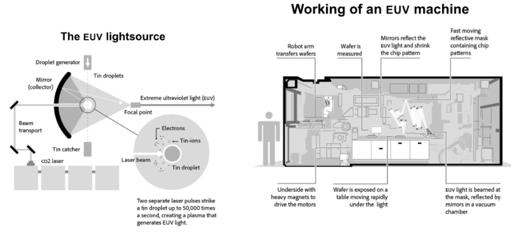
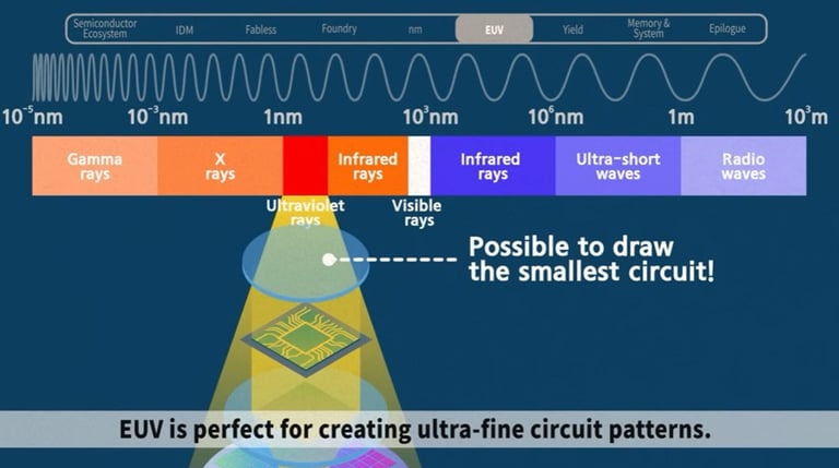
.How does EUV work ?
Great article from Qartr That shows just how important EUV is:
https://quartr.com/insights/company-research/asml-architecting-earths-most-complex-machines
I would sincerely advise to read the full article as it really goes in depth about ASML’s business model. It’s a great article that I would advise any ASML investor to read. As it really captures ASML’s MOAT
an extract from that article on The EUV part :
“The "commonly" used way to create EUV light is through a process called laser-produced plasma. In this process, you shoot a laser on a droplet of molten tin roughly 50,000 times per second, which creates a plasma that emits EUV light. The plasma generated during this process can reach temperatures of several hundred thousand degrees Celsius, which is multitudes hotter than the 5,500-degree surface of the Sun.
To be able to etch silicon wafers with EUV in order to produce chips, the light has to be directed through a series of precision mirrors, which focus and shape the beam before it illuminates a photomask containing the desired circuit patterns. The EUV light projects these patterns onto a silicon wafer coated with a photosensitive material, enabling the fabrication of intricate semiconductor features. According to Marc Hijink in his insightful biography FOCUS: The ASML Way, no single person fully understands every aspect of how these machines operate.”

As the article talked about FOCUS : the ASML way, I went ahead and read it. Great read by the way.
Here is an extract about EUV I find interesting :
« The Sun’s corona, 93 million miles away, is the closest place you can find extreme ultraviolet light in its natural form. On Earth, however, generating EUV requires extremely sophisticated technology. One way is to shoot a powerful laser beam at a tiny droplet of hot tin. This creates a plasma, an energy charged form of gas, far hotter than the surface of the sun. In this process, invisible light with a wavelength of 13.5 nanometers is emitted. If you can catch this with a mirror, you can direct it into a lithography machine to project a chip pattern. Sounds simple: you just have to build a sun.
Please, do be careful when you shake hands with Joann. She has the most remarkable fine motor skills, honed through years of work in ASML’s cleanroom in San Diego. Hunched over a machine in complete concentration, she carefully wraps two wires around what is known as “the nozzle”. That is what they call the spout at the heart of the EUV light source, responsible for shooting tin droplets through a hollow needle at a rate of fifty thousand times per second. Only Joann and one of her colleagues have the ability to wind and solder these virtually invisible wires. It’s a delicate task few could ever master. ‘Even watchmakers can’t do this,’ says their awestruck boss, ‘and there’s no way to automate it.’ It is not a trivial matter: the nozzle regularly gets clogged during day-to-day use in the chip factory. When that inevitably happens, the only thing to do is to swap it out for a new one. It’s hard to imagine, but without the fingers of Joann and her colleague, the EUV machines at Samsung and TSMC would grind to a halt. In the year 2023, two pair of human hands keep the world’s most advanced chip production lines in motion. »
Here is an interesting story also of how ASML had a lot of difficulty to make the EUV machines work at the start :
“Believe what you like about the Dutch, but ASML clearly has a leader: Martin van den Brink. ‘CEO’ might not be on his business card, but he’s without doubt the rock the company relies on. He’s the one setting the technical agenda, helping to write patents and determining the strategic acquisitions. It is his name that commands respect throughout the entire chip industry. And if one of his plans gets blocked in the boardroom, he’ll dig in and stick to it until he gets his way. When it comes down to it, it is clear who has his hand on the wheel. An autocracy with a hint of anarchy grew around Van den Brink, a culture in which everyone has the freedom to propose a better idea. As he said himself, ‘at ASML, you should have the feeling that you can change something. It’s the people that make the difference.’
But Martin van den Brink faced another challenge. He needed to immediately start looking for customers for the new machine, which at this stage was only a blueprint. In 2017, he arranged for a private tour of the Van Gogh Museum in Amsterdam so he could speak with the chip manufacturers among the sunflowers. But Samsung had no interest in a High NA machine. ‘Make sure you get the promised 100-watt light source up and running first. Then we’ll talk,’ the Koreans responded. At the end of that year, Wennink and Van den Brink flew to South Korea for a meeting with Kinam Kim, the head of Samsung’s semiconductor division. As they stepped off the plane, Martin glanced at his phone. Grinning like the Cheshire Cat, he showed the message to Wennink. It was an email from the Australian engineer Danny Brown, radiating relief: ‘We have 100 watts!’ San Diego had finally pulled through. But to truly convince Samsung, they needed to have an EUV light source fully up and running in Korea, not just in some shaky testing system on the other side of the world. And the collector, the mirror that captures the EUV light, was still getting contaminated far too often. That is simply not workable in a chip factory that needs to run around the clock. ‘So really, we did not have anything,’ said Van den Brink. He was never one to count his chickens before they hatched. One Saturday morning just before Christmas, Samsung’s technology chief arrived in Veldhoven. He wanted to see results. ‘You go on ahead,’ Van den Brink had to tell his wife. He was about to leave with his family on a ski vacation, but the light source was still malfunctioning. Desperate to find a solution, the technical director and his teams in San Diego held daily calls with Martin to solve the issue of the blackened mirrors. ASML had until March 2018 to get Samsung’s machine working, but there was no good news to give the visitor. Meanwhile, another deadline was fast approaching: Van den Brink had promised the supervisory board he would secure orders for the High NA machines before the first of the year, otherwise his plan would halt. A request for a three-month extension was made: one more quarter to decide the commercial fate of EUV. Van den Brink didn’t dare provide any guarantees about its success. He could already hear the smug analysts taunting him all over again. In the meantime, Intel was actually considering buying a set of High NA machines, but the asking price was half a billion dollars higher than what the Americans were willing to pay. Van den Brink’s jaw hit the floor. ‘Holy cow. Well, if you guys really want those machines, we’ll split the difference.’ Intel agreed, although the details still needed to be worked out. Van den Brink rallied his sales team; they needed to bulldoze this enormous financial hurdle as soon as possible, and with that he set off to Taiwan to reel in the next High NA customer. At first, TSMC showed no interest in this newest generation of machines. But when Van den Brink and Wennink flew together to Taipei in February, the Taiwanese were convinced. ‘It’s a leap of faith, but we’re jumping together,’ Wennink poetically promised them. That very line persuaded Morris Chang to purchase TSMC’s first EUV machines. And if the implementation of new technology proved a challenge, ASML would ensure that backup machines or alternatives were available to keep production going. Samsung proved to be a tougher case. The Koreans had been waiting seven years for a working EUV machine, and they were out of patience. Martin van den Brink wrote a personal email to Kinam Kim: ‘Give us one more month – just until April. Then it’ll happen.’ A completely coincidental discovery pushed EUV over the tipping point. In February 2018, an engineer noticed something strange: ‘Isn’t it odd how the mirror becomes clean again when we open the vacuum system to change parts?’ Antoine Kempen, a chemist on the team, had an explanation: it was likely because of oxygen entering. A rapid series of tests followed, and their suspicions were confirmed: if you add a bit of oxygen to the vacuum in addition to the hydrogen, the mirror of the light source stays functional far longer. At the end of March, Van den Brink traveled to Korea to show that EUV was ready for production. ‘We didn’t tell Samsung anything, only that the machine needed a tiny upgrade. One extra pipe with oxygen, and the problem was solved.’ Satisfied with the result, Samsung immediately signed the contract for the High NA machine.
The descriptions that chip manufacturers use for these technological generations or ‘nodes’ need to be taken with a grain of salt. The physical dimensions of the smallest circuits and connections on the chip are, in practice, five to ten times larger than advertised. A nanometer was once just a nanometer, but accuracy has never stopped a good marketing slogan. Neither does ‘EUV chip’ tell the whole story. Every processor is built in dozens of layers: if you cut a chip in half, you’ll uncover all sorts of different lithography techniques stacked on one another, just like the rings in a tree trunk. Only a handful of the layers with the most critical circuits are exposed using EUV. For the patterns of the other layers, conventional machines do the job.
whenever the laser was taken out for repairs, the whole operation would stand still for weeks, or even months. This meant a large number of back-up machines needed to be on standby at all times. Chip manufacturers are also keen to exaggerate problems with the machines. They cannot replace a multi-million-dollar scanner for a competitor’s version at the first sign of trouble, so instead they prefer to keep ASML on its toes by emphasizing the setbacks and presenting long lists of complaints. The engineers are bombarded with PowerPoint presentations containing hundreds of slides – one for each missing screw and each delayed spare part. But by far the most noise is made over contaminating particles that cause deviations on the silicon wafer. Issues here are quickly passed on to ASML specialists who can help optimize production. It is a stressful job, according to one of the employees in Asia. You’re meeting customers during the day, conferring with the designers in Veldhoven in the evening, and taking video calls from San Diego in the early morning. It feels like a non-stop meeting that leaves you with at best five hours of sleep per night. ‘Unless an unexpected problem arises. Then it’s even less.’ The mirror, which collects the light from the exploding tin droplets, requires regular cleaning. Initially, this task needs to be done every few weeks, eventually extending to every few months. ASML developed a carwash-like system, equipped with a high-pressure cleaner specifically designed for the collectors. With so many EUV machines already running in Asia, it is far more convenient to run this process in that region, rather than constantly having to fly the mirrors back and forward to the Netherlands to be cleaned. This is why Linkou, ASML’s Taiwan branch, cleans more than two hundred EUV collectors each year. Even the dirty mirrors from South Korea are sent to Taiwan, where they end up in Cathy’s cleanroom cabin. She’s just graduated as a mechanical engineer and is busy working on a new subject: a mirror with caked on blobs of tin, as if a sloppy painter had been messing around with putty. Cathy sets the timer: twelve hours of cleaning with CO2, and the mirror is ready to go back into a machine. The majority of mirrors find their way back into a scanner owned by the largest customer, TSMC. After all, Korea may provide the digital memory, but the world runs on the computing power from Taiwan.
However, in 2018 the new lithography machines were not working nearly as well as hoped. Mysterious particles that floated around in the machines were causing headaches and were decreasing the number of usable chips per wafer. And at TSMC, the yield is sacred: every fraction of a percent counts when you produce more than 15 million wafers annually, each containing several hundred advanced processors. Because the lines in EUV are so extremely thin, any amount of contamination has consequences. ASML keeps track of the number of errors that TSMC discovers in a ‘particles per week’ tally. The Taiwanese practically explode with anger if tin particles end up on the mask. The fallout is immense: any mistake there is repeated on every wafer, with every step of the exposure. It is possible to cover the masks with a protective film, or ‘pellicle’, which keeps the particles at a distance and unable to do any harm. Think of it like a smudge on your sunglasses that you can still see through. But no matter how thin, this extra layer will always block out some valuable EUV light, meaning it’ll take longer to expose the wafers. Every solution has its price in the world of ASML. Thanks to the new machines, TSMC no longer needs to use double or triple exposures to draw fine lines on chips, at least for the time being. This saves money and time, but the learning curve is steep. It’s not an exact science, but rather a matter of trial and error, and adjusting accordingly. They gather data on ‘wafer movements’ from an early stage, as their data analysts use this information to improve the yield. To fill the database faster, TSMC also orders as many machines as possible from ASML. This kills two birds with one stone: every machine in Taiwan means one less for a competitor in South Korea. Veldhoven has limited production capacity, especially for the latest generation of scanners, and chip manufacturers gladly take advantage of this shortage. »
an extract from that quarter article on The MOAT part :
“ In fact, ASML recently shared that 90% of all lithography machines it has sold over the last 30 years are still operational – pretty remarkable considering its complexity. Some remain in their original locations, while others, after reaching the end of their initial use, are refurbished and resold to other manufacturers. Even some of their old PAS 5500 systems are still churning out chips.
So, once installed, these machines can operate for decades, a crucial factor in an industry where the capital cost of building a cutting-edge fab is astronomical – usually exceeding $15 billion. In addition, ASML has mastered the art of keeping these machines not just running, but improving. They offer services to upgrade and enhance machines even decades after installation, and have service staff available 24/7 at every facility with an ASML machine in operation. This means that a machine purchased today can continue to become more efficient and productive over the next several decades. This ability to upgrade ensures that customers continue to see value in their investment, further incentivizing them to purchase from ASML and remain loyal for future needs.
The revenue model of ASML reflects this long-term relationship with their customers. New machine sales account for about 75% of ASML's revenue, with the remaining 25% coming from services and field options, including maintenance and upgrades. This diversified revenue stream also helps ASML maintain a steady income, even as the semiconductor industry experiences its inevitable cycles. This arguably also adds a razor-razorblade touch to ASML's business model. Additionally, training ASML's service staff is a highly specialized process that takes around two years, further contributing to the complexity of their operations and bolstering the company's competitive advantage.
The semiconductor industry has historically been very cyclical, and ASML's experience is no exception. However, in recent years, these cycles have become less severe for ASML. One reason for this is, as previously addressed, the company's unique position as the sole producer of certain types of lithography equipment. If a manufacturer such as TSMC wants to build the next generation of chips, they have to go through ASML. And with no competitors to turn to, manufacturers are hesitant to cancel orders, even in tough economic climates, because they know they'll lose their place in the queue when demand picks up again”
So, if you're a customer, like TSMC for example, and you have a 30 to 40 year track record of working with ASML, and the machines that you purchased 30 years ago are still working and producing chips for you today. Then, what would make you want to risk that relationship and potentially go with a competitor ?
Where, you don't know if their machines are nearly as good. Imagine a brand new competitor comes to market tomorrow and they can offer ASML machines, even at a slight discount, if you're TSMC and you have that 30-year track record with ASML and their machines are so critical to your business and they've done a great job executing, their machines just work.
You have that relationship, are you really going to sacrifice that relationship and that historical track record of working together to try out a competitor ?
When you also don't really know the competitor's quality of their machines and it's a brand new machine to Market.
When you have that long track record with ASML and you know the quality of their machines, because these machines are so vital, they are so important to these ship Fabricators.
Here is an example I found in FOCUS : The ASML way :
« The approach here between the lithography manufacturers differs wildly. ASML’s machines still require extensive remedial work, while ASML’s competitors in Japan always aim to deliver machines the same way they deliver their cameras; finely tuned, and ready for immediate use. You just need to plug it in. The latter may seem the obvious choice, but ASML’s ‘perfect enough’ approach has its advantages. With this method, the chip manufacturer can begin their own testing much quicker, allowing them to fine-tune the device to the particularities of their environment and get it on its way to fulfilling its purpose: exposing wafers all day, every day. And that’s a different ball game.
But as soon as there’s a malfunction the stream stops, leaving the machines standing like a line of impatient motorists on the wrong side of a traffic accident. A blockage like this is critical: the heart of the factory, the lithography machine, can no longer beat. On a normal day, the quickest devices usually spit out two or even three hundred wafers per hour, and one wafer of chips can fetch up to 250,000 dollars. To a chip manufacturer, their actual heart may as well be on the line when a scanner stands still. Todd Garvey is one of nine thousand customer service employees working around the world to keep lithography machines ticking. Operations are run from their base in Arizona, home to ASML’s American office since 1984. The cleanroom uniform is a dust-free bunny suit that leaves only the eyes exposed. It wouldn’t be out of place in a hospital, and neither would Garvey. He sees himself as one of ASML’s nurses, tending to his patients throughout the day and night. Service engineers like Garvey are responsible for keeping a fleet of forty to fifty machines in the air. It takes years to qualify for this, and this is why ASML starts training maintenance staff long before construction on a new fab begins.
Walk into any cleanroom, and you’ll find the lithography machine is always king. The most expensive tool is also responsible for the most critical part of the production process, so it’s vital that it’s kept running at full power at all times. The other machines are less of a strain on the wallet and handle the rest of the steps, such as etching, heating, and applying new layers to the wafers. In between all this, the discs are also constantly measured to check the layers of the chips are still properly aligned. Lithography machines will work between 98 and 99 percent of the time if they receive regular maintenance. Just like on a highway, with planning you can easily minimize disruption by redirecting tasks and traffic to other production lines. It’s the crashes, the unexpected ‘tool down!’ warnings that deliver the most economic damage. And no siren will sound to tell you. They’re usually disconnected: there’s enough noise in the factory as it is. If a malfunction is expected to last more than 48 hours, it is better to switch the wafers to a different production line and take the reduced yield on the chin. This leaves the robots waiting patiently in line while the ASML employees scramble to diagnose and revive the patient.
Wim Pas remembers his white whale clearly. The site manager for the TSMC fabs north of Phoenix ran into trouble with a notorious immersion device; it would inexplicably produce faulty chips for two hours after every restart, and then run seamlessly as if nothing had happened. It took months of research to figure out why. The second the machine stopped, five droplets of water would fall on a layer of glue, causing it to expand by just a few nanometers. This was all it needed to throw off the chip-pattern. And once the moisture evaporated, the glue would shrink, leaving no trace of any error with the machine. Problems like this only come to light in the harsh reality of the factory floor. Even with years of meticulous planning, half the issues these machines face could never be imagined. This is exactly why ASML leaves the fine-tuning of the design for when the engines are running. It is also the only way to find which parts wear out too quickly. As Pas says, ‘It’s only here that everything wrong with the design reveals itself.’ Then you have to hope the spare part is available – with a device comprised of so many different components, it’s almost impossible to predict and prepare in advance for what will be the first to go.
Unforeseeable complications aren’t limited to the mechanics of the machines. Despite their best efforts, the cleanrooms can’t always keep the outside world at bay. Earthquakes and atmospheric pressure fluctuations due to thunderstorms can easily disrupt the lithography process. Or cows. Intel once faced an inexplicable drop in yield every night for a few hours, with researchers running in circles until they finally realized the cause: cow farts. Every night between 1 and 2 a.m. the wind would change direction and methane gas from nearby dairy farms found its way into the cleanroom through the air purifiers. The extra gas from their sleeping neighbors was enough to affect production and dropped the percentage of flawless chips produced in this time window. Filtering the gas wasn’t possible, so Intel had to pay for three farms to relocate. Since then, everyone scouting a location for a chip factory knows to keep an eye out for cows. »
To actually create semiconductor chips, it is such a crucial part of their business that I think they would pay a premium just for security with ASML business.
So, I think, that ASML is just so entrenched in the industry at this point that even if a competitor came, I don't think their customers would switch that easily.
So, how is ASML going to be disrupted that's my question ?
okay so now let's move on to ASML potential competition because Canon is still trying to compete.
But Canon and Nikon gave up on the EUV machines, they're not trying to build them anymore but they went down a different path called Nano imprint lithography which essentially can create the same type of semiconductors as ASML machines, it just does it in a different way.
Here is an article talking about this.
So, they essentially branched off and built a completely different technology that can still achieve the same thing, at least that is what Canon is trying to say. Canon has collaborated in development with the US startup “molecular imprints Inc” before acquiring the company in 2014 after nearly 20 years of research and development Nano imprint lithography machines emerged receiving positive reviews from industry experts. Canon also claims that nano printers are simpler and cheaper than the traditional EUV lithography machines consuming only 10% of the energy of EUV machines due to their use of optical pattern imprinting technology instead of lasers for circuit pattering on Wafers with its trailing advantages nano imprint technology is assessed to be capable of producing semiconductor chips at the 5 nanometer process node even progressing towards 2 nanometer with this Advanced Technologies. So, continuing on this says Canon ships its first Nano imprint lithography machine Rivals ASML’s and this was back in October of 2024.
So, just a couple of months ago, although Canon has not made the price of its machines public when the company first unveiled the technology the CEO said the price would be one digit less than ASML EUVs. the latest version of Netherlands based ASML's High NA EUV machines currently retail for approximately 370 million.
So, Canon's new machines are said to be on a digit shorter or cheaper than ASML machines which means that they'll be in the tens of millions of dollars range.
They're not going to be in the hundreds of millions, so this could potentially be a 10x improvement over ASMLs machine price.
So that's a pretty massive Improvement in price, if you are a current customer of ASML and you could get a Canon machine for a tenth of the price then that could start to disrupt ASML if these machines are actually high quality and again this was released on October of 2024.
AND, this was Canon's first Nano imprint lithography machine sale, so we're going to have to see how this plays out.
So, Why am I not worried about Canon's nano imprint machines ?
Well, If they're cheaper and they can produce the same level of quality in a chip fabrication then why aren't more customers buying them ?
Why aren't these things flying off the shelves ?
so here is another article I found about this :
“while the company has developed its Nano imprint lithography technology. Since 2004 it has not taken off in the world of increasingly complicated ships that's partly because the EUV machines like those made by ASML have worked better during the chip printing process.”
So to put it simply, it sounds like ASML machines just work better and are more reliable.
“Many challenges face the technology before it can be broadly adopted, there are still concerns about minimizing defects from dust particles during production. For example, Canon will also need to collaborate with other companies to create materials compatible with this new lithography method which will be essential for widespread industry use.
Finally, this technology is incompatible with flows involving DUV or EUV making it very challenging to integrate into existing manufacturing flows. Chipmakers will have to design their Production Technologies around the technology which is both expensive and risky. “
So, basically with the way that the supply chain and Manufacturing flow works today is on DUV or EUV lithography machines which are provided by ASML.
So, for a company like TSMC to come in and try out CANON’s machines, they would have to revamp their entire manufacturing process which would be a massive investment and it would be risky because these are brand new machines that so far seem like they're not as reliable.
So, for a company like TSMC would they really want to make that big of a bet on these new machines just to save a little bit of money when it is extremely risky and it's not really a proven technology yet ?
Furthermore the relationship between ASML and TSMC goes deep, here is an extract from the book FOCUS: the ASML way :
« In 1987, the company was contacted by Morris Chang, former technical director of the US company Texas Instruments. Raised in China and educated in America, Chang was an expert in increasing the yield, the percentage of faultless chips on a wafer. The Taiwanese government noticed and tapped him to be the lead in establishing a national chip industry, promising to cover any and all costs. This marked the start of the Taiwanese Semiconductor Manufacturing Company, or as it is widely known today, TSMC. Chang sought another large, experienced investor from the sector. But the Japanese were not interested, plus talks with Intel and Texas Instruments fell through. So he turned to Philips, in his eyes the cream of the second-rate chipmakers. Hardly a compliment, but what mattered was getting the collaboration – and Philips was the next best thing. Philips happily agreed, taking a 28 percent stake in TSMC and sharing the expertise cultivated from the Mega Project. But the partnership also opened the door for ASML to get their machines onto TSMC’s factory floors. Chang held fire. He needed to be convinced of the quality of the equipment. While on holiday with his wife in Bali, Wim Troost received a polite tap on his shoulder. ‘Mr. Troost, a call for you.’ He wormed out of his cross-legged position in the middle of a dance performance and snuck out of the audience to take the call. It was Veldhoven: the deal with TSMC had come through. It turned out there was a way to win Chang over. Troost had given away the first machine to TSMC for free on a no cure, no pay basis. The highly demanding Taiwanese were convinced. With the partnership between TSMC and ASML in full swing, the Taiwanese chip industry proceeded to boom. The two companies turned out to be surprisingly likeminded. Both functioned in an equally speedy and chaotic manner, with each totally dependent on the other to churn out endless piles of wafers every hour, free of faulty chips. ‘We have their backs and they have ours,’ was the mantra of the ASML’ers. This one sentence became the formula for dominating the chip market. »
One of the primary concerns with the FPA 1200 NZ 2C is it's through throughput or the number of Wafers it can process per hour. traditional photo lithography machines particularly those using DUV or EUV technology have established a high throughput that Nano imprint lithography like Canon systems has yet to match.
the lower throughput means that production lines would require more machines or more time to produce the same volume of chips which can be a significant drawback for large scale manufacturing.
So, what this first point is basically saying is that while Canon's machines may be one 10th of the price for a manufacturer. To actually produce the same amount of chips they would need more of them.
So, if one of ASML machine may produce 100 chips per minutes, whereas one of Canon machines may produce 10 chips per minute and therefore for the customer to be able to produce the same amount of chips they would need 10 Canon machines and at that point are you actually saving any money ?
The answer is no, so the throughput issues are actually causing Canon’s machines to not take off.
On to point number two, defectivity and precision Nano imprint lithography involves direct contact between the mask and the wafer which inherently increases the risk of defects from particles or imperfections on the mask.
while Canon has developed environmental control Technologies to manage contamination. The defect rate is still a concern compared to DUV and EUV lithography. Precision in alignment and overlay crucial for multi-layer Semiconductor fabrication also presents challenges, as noted by experts in the field.
So, overall the output quality is a concern for these new machines and if you're TSMC and you're trying to stay on The Cutting Edge, quality is everything, you cannot sacrifice your quality because if you sacrifice quality then you're not staying on The Cutting Edge anymore.
Therefore, I don't think that these companies are going to widespread adopt Canon’s machines.
So, these are all major barriers to entry for a competitor like Canon to even try and attempt to take on ASML.
And now?
The progress is far from over, as there is still potential to further improve the minimum resolution achievable with EUV for ASML. Which would create even more distance between ASML and their competitior.
How?
Just like with immersion lithography, the key to improving resolution is to increase the numerical aperture (NA). By doing so, EUV can continue to push the boundaries of chip miniaturization, allowing for even smaller, more powerful transistors and further enabling the future of semiconductor technology
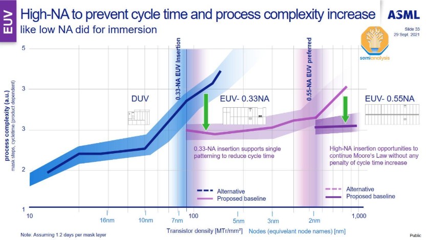
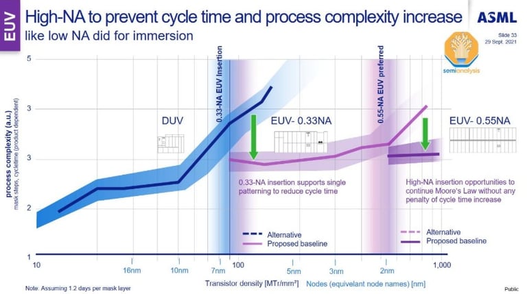

That’s why today, we are talking about two types of EUV machines:
EUV Low-NA: This refers to the NXE family of machines, which have a numerical aperture (NA) of 0.33. These are the most widely used EUV machines today, delivering impressive capabilities for advanced chip production.
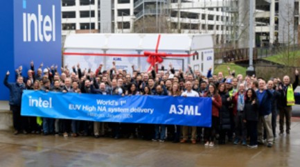
EUV High-NA: This refers to the EXE family of machines, which feature a higher numerical aperture of 0.55. These are the most advanced EUV machines available, but they have yet to find widespread market adoption. Only a few machines have been delivered to Intel earlier this year, as they are still in the early stages of implementation.
The transition to EUV High-NA is expected to unlock even greater resolution potential, but there are still hurdles to overcome before they can be fully integrated into mass production across the industry.
Here is a link that quickly shows high NA technology :
I also put under a passage from FOCUS : the ASML way :
« The light is bounced throughout the entire EUV system: first from the light source to the mask, then from the mask to the silicon wafer. Each mirror absorbs 30 percent of the light rays, and the new High NA machine has two mirrors fewer than the first version. This effectively means more light and a faster exposure, which saves valuable time for the manufacturer. So why not make a machine with these large mirrors in the first place? As Van Schoot explains, ASML does not like to jump straight into the deep end. ‘The equipment for measuring mirrors is getting increasingly complex. Each time we ask ourselves how far we can push it and how much risk we’re willing to take. With the first optics, we took it as far as we could with the available technology.’ Chip manufacturers also need to be able to keep up the pace. The area in which the light beam is razor sharp is now slightly smaller on the new system. Think of a portrait photographer who only brings your eyes into focus and leaves the rest of your face blurred. As a result, deviations on the surface of the wafer require extra attention, and the layers applied by other chip machines need to be even thinner. Another problem: the EUV light falls at a steep angle on the mask in a High NA system, causing only a small fraction of the pattern to be properly reflected. An anamorphic or ‘widescreen’ mirror is used to fit more patterns on the mask, but the field of view is smaller and the chip design has to be adjusted to accommodate this. And then there’s ‘dead time’, ASML’s morbid term for the valuable seconds when the wafers are not being exposed. The speed of the wafer tables has been ramped up to cut this down: they now accelerate to their position under the light with a force more than ten times that of gravity. Faster than a fighter jet. This is not even the quickest part of the machine – the mask with the original chip pattern moves four times as fast. To keep these forces in check, a counterweight races in the other direction. This combination of brute force and atomic precision is controlled by software. Computing power is also needed to calculate the positioning of the mirrors, with a series of sensors constantly monitoring how they behave and how this affects the image on the wafer.
In a nearby room, robots practice with dummies to pre-program the movements. The actual High NA mirrors are already in the making, albeit in various stages of completion. It takes an entire year to fabricate and perfect a single mirror. The entire system of mirrors will soon end up in the ‘optical train’. The complete lithography machine is an awe-inspiring monolith, as tall as a two-story house and filled with futuristic technology. The cleanroom also needed to expand to accommodate the sheer size of it. You can tell from looking at the Zeiss campus where the High NA optics are assembled – it’s the tallest building in the area. Zeiss itself has roughly a thousand employees working on the new technology. Regular meetings with ASML help to keep the collaboration running smoothly.
You may think a lithography machine with a price tag of hundreds of millions of euros would be able to make perfect copies of chip structures. Think again. The mask, which carries the original image of the chip, does not leave an exact replica on the photosensitive layer. The chemical processes that occur on the wafer create rough and messy lines. However, with mathematical models, you can calculate how to shape the mask so that, despite these deviations, a pattern emerges that will transmit the electric signals on the chip without fault. You can compare it to the beauty filters on TikTok or Instagram, which correct the ‘imperfections’ on your face to make you look like a model. However, making a mask takes much more time than snapping a selfie, and it takes weeks for the pattern of the chip to be converted into a flawless image. Computational lithography, as this technology is called, is an indispensable link in the production of chips. Martin van den Brink knew this when he charted out ASML’s long term strategy in the late ’90s. As chips become smaller, so does the room for error, and at a certain point using software to make these adjustments is the only way to keep producing chips that work. The Dutch company gathered the required expertise through a series of acquisitions. In 1999, they took over American start-up MaskTools, and in 2006 ASML paid over 270 million dollars for Brion, a company with branches in Silicon Valley and China. Brion developed software that simulates the operation of lithography machines to create masks. The production of a complex EUV-mask costs more than half a million euros and takes a huge amount of time to calculate. If you use smart software to accelerate this development, you save yourself a lot of money. ASML also developed its own measuring instrument, the Yieldstar, which traces errors on wafers with a camera. And in 2016, it bought the Taiwanese company HMI for 2.75 billion euros. Their machines check the wafers by taking random samples with an electron beam. Each of these applications generates vast amounts of data, all of which is then stored on large computer systems in the chip factory itself. It’s a vicious cycle: more computing power is needed to design and manufacture chips for more powerful computers. Silicon Valley is the birthplace of the semiconductor industry, yet the last major chip factory in this region closed its doors in 2009. However, the specialists in chip software remained in California and soon found their place among the new tech giants. ASML Silicon Valley is located on West Tasman Drive in San Jose. Brion’s and HMI’s Asian origin is immediately noticeable by the giant dragon made out of balloons in the lobby, positioned proudly next to the wall displaying the company’s patents. Chinese New Year is an important holiday here, as is the Dutch celebration of King’s Day on April 27. Just to make sure, the ASML’ers also celebrate Cinco de Mayo. Yu Cao, the co-founder of Brion, thinks it fosters a sense of community. ‘Silicon Valley’ is different to the other ASML locations. Eric Meurice, the CEO who signed the acquisition of Brion in 2007, urged the founders not to let Veldhoven control them too much: ‘If ASML tries to push you into their corporate structure, ignore it. And otherwise, just give me a call.’ Veldhoven has a rigid project organization entirely focused on building scanners, and this does not match how HMI and Brion operate. Brion supplies its optical proximity correction software, or OPC, to companies that are also located in San Jose like Samsung and GlobalFoundries. The measuring technology of HMI faces far more competition than ASML’s lithography systems do. But when put together, these three elements – measuring technology, correction software, and the scanner – form the pillars of ‘holistic lithography’. It is an ecosystem carefully built by ASML to reduce the margins of error throughout the chip factory and increase its effectiveness. The applications division, as this branch is known within ASML, now generates billions in revenue.
The scientists from Delft are now collaborating with San Jose on a radically enhanced version, slated to be ready by 2025 and capable of handling the unbelievable amounts of data required to inspect the wafers in detail.
The explosion of measurement data has made it impossible to capture all the variables at play into predictable formulas. Therefore, Brion uses AI to understand the interplay between the light beam, the mask, and the chemical reactions on the wafer. The technique used for this is machine learning, in which neural networks look for patterns in an enormous set of data. In machine learning, the computer draws conclusions that you can’t replicate. The software can even predict in advance how you should set up a lithography machine to get the best results, prompting Martin van den Brink to coin a term for it: voodoo software. ‘No one knows exactly what goes on with machine learning’, he expresses. ‘But if you rely solely on AI, you’re not adding any extra value. Then you don’t need to understand what it’s doing anymore, and that’s where the problems start.’
‘Martin hates laziness,’ clarifies Jim Koonmen, the head of operations in San Jose. ‘He can’t stand it if you say, “I can’t make sense of the model, so I’ll just train a computer and hope for the best.” He challenges the people here: why do you choose machine learning over modelling that uses the physical principles?’ Overdependence on dark magic is risky: if you do everything with voodoo software, you’ll no longer differ from your competition. Van den Brink sees it as a valuable addition, but only as a final step to speed up reaching a solution. ‘We need to distinguish ourselves. If we don’t include the added value of our physical models, then anyone can do it.’ He compares it with generative artificial intelligence, such as ChatGPT, which can create readable text in seconds, but doesn’t add anything new. ‘As if you asked ChatGPT to write a book about Martin van den Brink,’ he says. Ultimately, the software from San Jose is the glue that binds all the components of the machine together: without it, one would never be able to optimally align the lighting system, the mask and the lens. But software has its drawbacks. Top of the list: it is easy to copy. In 2014, six former Brion employees made off with trade secrets, stealing – among other things – two million lines of software code, algorithms and manuals via email and used the details to start a competing company in Silicon Valley. When Samsung wanted to terminate its contract with Brion because a new competitor with a suspiciously good product had emerged, alarm bells sounded at ASML. This new company was called Xtal, pronounced ‘crystal’.
When the judge and jury then examined the Xtal code behind closed doors, it became evident that algorithms had indeed been copied. ASML was awarded 845 million dollars in compensation in 2019. But with Xtal long bankrupt, there was nothing to recover. The high amount was intended as a deterrent, a serious signal for anyone else considering sneaking off with trade secrets. Incidentally, Xtal founder Yu Zongchang started a Chinese counterpart around the same time. His company, Dongfang JingYuan Electron, is still in business and even receives subsidies from the Chinese government. ASML urged its customers to steer clear of Dongfang, yet leadership decided not to publicize the lawsuit. After all, they thought, it involved less than 1 percent of ASML’s revenue, and both the stolen information and the contract with Samsung were safely secured.
You cannot produce a good chip without high-quality etching machines, measuring equipment and devices to apply the wafer-thin layers. And for all these you need supplier like Applied materials, LAM research and KLA. »
ASML Activities
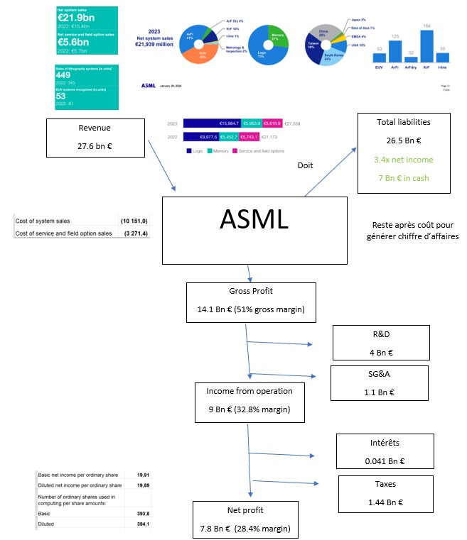
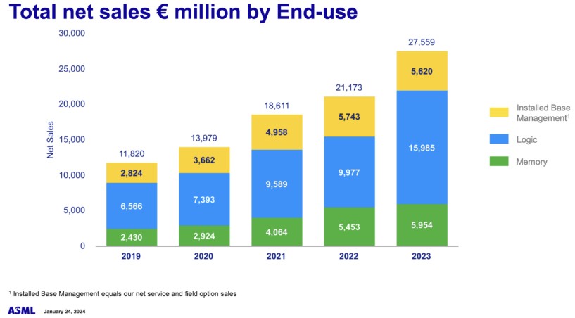
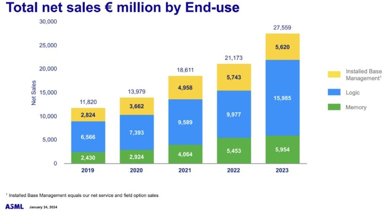
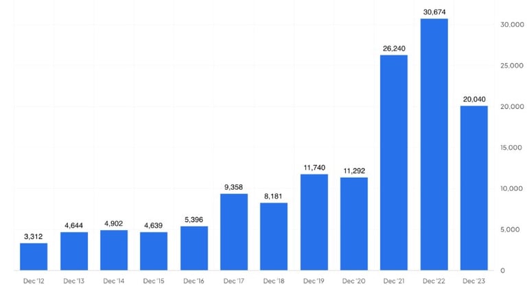
In 2023, ASML generated a revenue of €27.56 billion. This revenue can be broken down into two main activities:
Sale of Lithography Machines of All Generations: ASML continues to sell various types of lithography machines, including the I-Line machines. These machines are used for different types of semiconductor production, including advanced and older node processes.
Sales of Metrology and Inspection Machines: While this is not ASML’s core business, they offer machines for metrology and inspection. This segment competes with KLA Corporation, the current leader in this field.
Maintenance and Upgrades for the Installed Base: ASML’s machines have a long lifespan, so maintaining and upgrading their installed base is an important part of the business. This service segment is cyclical; when machine sales are high (during a peak cycle), the service revenue share is lower, and when sales drop, the service revenue increases.
A key point is that service revenue is expected to grow steadily as the installed base of machines continues to expand. Additionally, this service segment carries higher profit margins compared to the sale of machines, which further strengthens ASML’s financial position over time.
Sales Cycle of ASML
ASML’s systems are not delivered overnight. From the moment a customer places an order, it typically takes anywhere between 10 months (at a minimum) and 18 months before the system is delivered. This extended lead time is due to the highly complex and specialized nature of ASML’s lithography machines, which require precision manufacturing and thorough testing before they are ready for use in semiconductor production.
Like many industrial companies, ASML’s future revenue can be estimated based on its order book (the backlog of orders). As a result, it’s possible to anticipate the company’s revenue for the following year by analyzing how many orders it has in progress.
For example, based on its strong order book, ASML’s 2023 revenue was notably high, as expected. However, as predicted, 2024 saw a slowdown in revenue, aligning with the cyclical nature of sales in the semiconductor equipment industry, which is highly dependent on customer demand and investment cycles in semiconductor manufacturing.
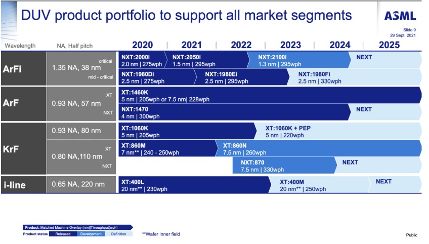
Breakdown by Type of Machines Sold
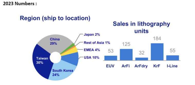
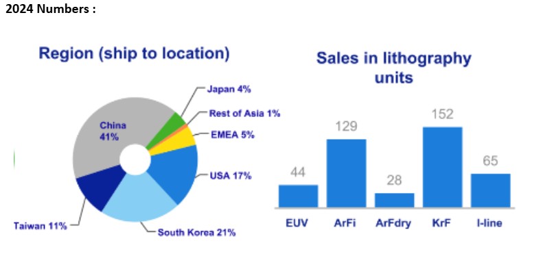
When analyzing ASML, it’s a common mistake to assume that they only sell EUV machines. In 2023, EUV machines actually accounted for only 42% of the total machines sold.
The majority of ASML’s sales still come from immersion and DUV (Deep Ultraviolet) lithography machines. This category includes :
ArFi (ArF Immersion) systems
ArF Dry systems
KrF (Krypton Fluoride) systems
These older technologies are still in high demand due to their role in producing chips with nodes that are larger than those produced by EUV, but are still critical for many applications in semiconductor manufacturing.
Thus, while EUV is crucial for advancing the smallest node sizes and most cutting-edge semiconductor production, the broader market for immersion and DUV systems continues to make up a significant portion of ASML’s business. This diversified product offering allows ASML to maintain its strong market presence across different segments of the semiconductor industry.
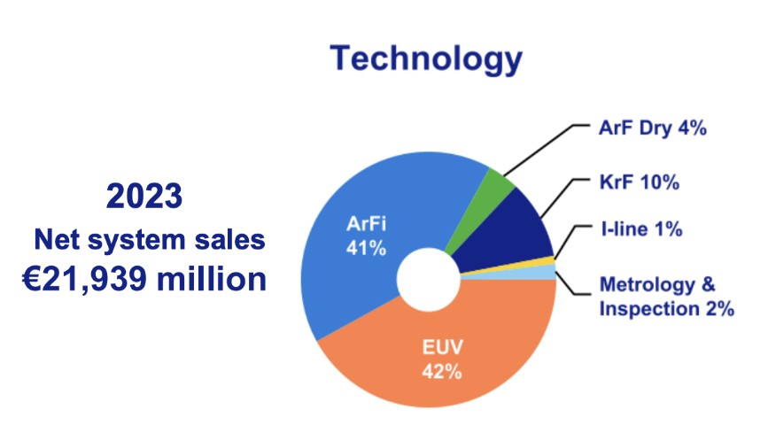
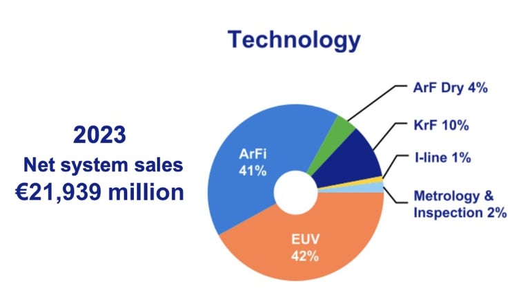
Sure, these numbers are volatile from year to year, but they clearly demonstrate the importance of less advanced technologies, on which ASML still faces competition, even though in reality, they still dominate this market.
Moreover, machines of all generations are continuously improved to increase their productivity and enhance their precision, making them more attractive.
The innovation cycle in the sector typically works like this: a new machine is released that reduces the minimum resolution with acceptable thresholds for yield and productivity. Then, over time, ASML improves the other parameters. In this regard, EUV also fits in. Due to its complexity, it is capable of processing fewer wafers per hour than the best DUV machines.
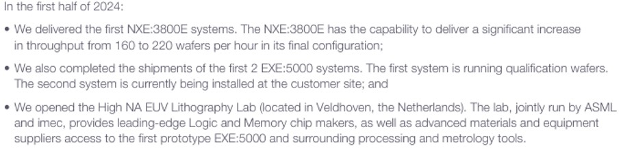
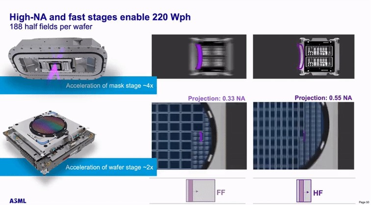
In the latest call, the new CEO, Christophe Fouquet, mentioned that customers have switched to the latest versions of the EUV Low-NA machines because they are able to increase the exposure throughput.
“Regarding our Low NA technology, we continue to ramp up the NXE:3800E system this quarter, with EUV customers now rapidly transitioning to this new model due to its superior performance, including more than a 37% improvement in throughput compared to the NXE:3600D.
We have now demonstrated a throughput of 220 wafers per hour with the new overlay record in our factory, and we are on track to deliver a system with complete specifications, with shipments of new systems and upgrades starting early next year.
As customers move to the NXE:3800E, the majority of Q4 deliveries are related to NXE:3800E systems.”
Christophe Fouquet – PDG of ASML – Call of Q3 2024
In terms of deliveries, DUV machines remain the primary systems shipped to customers in terms of volume.
Of course, the prices are not the same. Here are the estimates I found:
ArFi machine: Between €50 million and €80 million per machine
EUV Low-NA: Between €120 million and €200 million per machine
EUV High-NA: Between €350 million and €400 million per machine

Of course, to justify these prices, ASML needs to offer a certain added value to its clients. Since there’s always room to improve the minimum resolution through other processes rather than simply reducing the wavelength.
Clients
ASML’s clients can be counted on the fingers of two hands.
Indeed, semiconductor manufacturing requires a high level of capital investment: around $20 billion for the most advanced factories.
Here are ASML’s main clients and their share in ASML’s sales over the last 12 months:
TSMC (logic chips) : 28%
Samsung (memory chips) : 22%
Intel (logic chips) : 10%
SMIC (Chinese player, logic and memory chips): 3.5%
Micron (memory chips) : 2.7%
SK Hynix (memory chips): Not Classified (N/C)
Of course, these figures can change quickly depending on the orders. For example, Intel’s 10% share may decrease in the upcoming quarters due to the challenges they are currently facing.
Competitive Advantages
As we’ve seen, ASML’s main competitive advantage is its monopoly on EUV and its near-monopoly in the broader lithography field.
However, a monopoly, especially in the tech sector, can be lost quickly. While it’s possible, I believe this is a very unlikely scenario in the medium term for two reasons:
ASML’s corporate culture and unique organizational model
The structure of the lithography market
Let’s dive into each of these points :
Corporate Culture and Organizational Model
The fact that ASML won the race to EUV is no accident. Despite having far fewer resources than the market leaders of the time, several factors explain their success.
First and foremost, unlike Nikon and Canon (and Japanese and Korean companies in general), ASML made the decision not to vertically integrate.
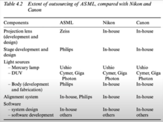
ASML didn’t win the EUV race by chance. Despite having fewer resources than the market leaders at the time, its success is based on several factors.
First, unlike Nikon and Canon (and Japanese and Korean companies in general), ASML chose not to vertically integrate.
This means that ASML relies on a multitude of ultra-specialized subcontractors to produce each component of its lithography machines. Similar to Airbus, ASML focuses on design, orchestration, and assembly.
This model proved to be a decisive advantage in the race to EUV:
Each component requires specific expertise. Developing all these competencies in-house would have dispersed ASML’s efforts and slowed its development. By outsourcing, the company could rely on the specialized expertise of its partners. For example, for the lenses, one of the key components, ASML collaborates with the German specialist Zeiss. Nikon and Canon, on the other hand, produce everything in-house, which dispersed their resources and energy.
Here are the Key Suppliers and Vendors for ASML :
1) Carl Zeiss AG
Role : Optics
Details: Zeiss provides the precision optical components essential for ASML’s lithography systems, including lenses and mirrors used in the EUV lithography machines.
2) Trumpf GmbH + Co. KG
Role : Laser Technology
Details: Trumpf supplies high-powered laser systems that are used in the generation of EUV light.
3) Cymer (a division of ASML)
Role : Light Sources
Details: Cymer provides the light sources for ASML’s lithography systems, particularly the excimer lasers used in DUV lithography.
4) Jabil Inc.
Role : Manufacturing Services
Details: Jabil offers various manufacturing services and components used in ASML’s photolithography equipment.
5) ASMI (ASM International)
Role : Deposition Equipment
Details: Supplies advanced deposition equipment used in the manufacturing process.
6. Edwards Vacuum
Role: Vacuum Pumps and Abatement Systems
Details: Provides vacuum and abatement solutions necessary for the EUV lithography process, which requires vacuum conditions.
7. IMEC
Role : Research and Development
Details: A key R&D partner, IMEC collaborates on advanced lithography research and development.
8. MKS Instruments, Inc.
Role: Gas Control Systems and Components
Details: Supplies critical gas control systems and components used in the photolithography process.
9. Pfeiffer Vacuum Technology AG
Role : Vacuum Solutions
Details: Provides advanced vacuum technology solutions for ASML’s lithography systems.
10. TNO (Netherlands Organization for Applied Scientific Research)
Role : Research and Development
Details: Partners with ASML on various R&D projects, particularly in developing new lithography technologies.
11. VDL ETG (VDL Enabling Technologies Group)
Role : High-precision Manufacturing
Details: Provides high-precision mechanical components and modules.
12. ZEISS Semiconductor Manufacturing Technology (SMT)
Role : Optical Components
Details: Another division of Carl Zeiss, SMT focuses specifically on components used in semiconductor manufacturing.
13. Coherent, Inc.
Role : Laser Sources
Details: Supplies laser technologies that are integral to the functioning of photolithography machines.
14. Nikon Precision
Role : Alignment and Metrology Equipment
Details: Provides metrology equipment critical for ensuring precision in photolithography.
15. SUSS MicroTec SE
Role : Photomask Equipment
Details: Supplies photomask processing equipment.
Notable Mentions
While the above companies are among the most significant and publicly acknowledged, ASML’s supply chain is extensive, involving numerous other suppliers and vendors for various components, from electronics and software to mechanical parts and chemicals.
Summary
ASML’s supply chain includes a wide range of companies specializing in optics, laser technology, vacuum systems, precision manufacturing, and research and development. Key partners like Carl Zeiss AG and Trumpf GmbH are particularly crucial due to their contributions to the core technologies that enable ASML’s advanced EUV lithography machines. Understanding the full scope of ASML’s suppliers highlights the complexity and collaborative nature of developing state-of-the-art semiconductor manufacturing equipment.
Here is a story I found about Zeiss in FOCUS: the ASML way
« The value of High NA lies in its ability to print chip structures with a precision of 2 nanometers and smaller, a reduction in scale made possible by the higher opening angle of the lenses. In technical terms: the numerical aperture (or NA) increases from 0.33 to 0.55 – the difference between Low NA and High NA. ASML’s suppliers have been working on parts for this new machine for years. Zeiss needed to begin production early on due to the extensive preparation demanded by lens fabrication. This prompted ASML to take a stake in Zeiss in 2016, which used the investment to kickstart the research process. It took five years to figure out all the ingredients required. Zeiss’s advanced laboratory sits between the mountains in Oberkochen, constructed on a thick layer of vibration-free concrete. There, with the help from ASML, the lens maker developed the measurement technology needed to manufacture the new mirrors. EUV mirrors are not flat like the mirror in your bathroom. They have complex shapes – think of the distortion you get from a mirror at a funfair. The difficulty is being able to measure whether the surface is smooth enough all around to reflect the light without disturbance. ‘If you can’t measure it, you can’t make it,’ as the Germans say.
For months, the surface is polished by robots, after which Zeiss shoots off the remaining atoms one by one. More than fifty ultra-thin reflective layers are then applied, and the mirror is ready. ‘If you lined it up right, you could hit a golf ball on the moon with one of these,’ says Thomas Stammler. And he has more comparisons: if you could stretch the mirror from a High NA system until it was the size of Germany, the largest irregularity would protrude at most 20 micrometers from the surface. That’s less than the thickness of a single human hair. It is perfectly normal to feel dizzy in this place. Not because of the sterile air, but because the mere thought of the extremely complex tools needed to make the chips destined for the phones of the future can make you lightheaded. A machine invented in Veldhoven, manufactured with parts from all over Europe and shipped to chip factories in Asia and the US, where it produces silicon wafers full of processors and memory chips that, in just a few years, will end up in the palm of your hand. »
Major Global Suppliers:
1. Carl Zeiss AG: Provides critical optical components, including lenses and mirrors essential for ASML’s lithography systems.
2. Trumpf GmbH + Co. KG: Supplies high-powered laser systems crucial for generating EUV light.
3. Cymer (a division of ASML): Provides the light sources for ASML’s lithography systems, particularly excimer lasers for DUV lithography.
4. Neways Electronics International N.V.: Supplies electrical control units, power controls, and wiring systems for ASML’s lithography products.
5. VDL Enabling Technologies Group (VDL ETG): Provides high-precision mechanical components and modules.
6. Edwards Vacuum: Supplies vacuum and abatement solutions necessary for the EUV lithography process.
7. MKS Instruments, Inc.: Provides critical gas control systems and components.
8. Pfeiffer Vacuum Technology AG: Provides advanced vacuum technology solutions.
9. ASMI (ASM International): Supplies advanced deposition equipment.
10. IMEC: Collaborates on advanced lithography research and development.
2) Outsourcing allows ASML to be more flexible. They distribute the investment burden among their various subcontractors, which enables them to explore different technological developments. While Nikon had to make choices that turned out to be poor, ASML could play on multiple fronts before focusing on EUV, as this technology showed a higher probability of success.
3) The power dynamic is extremely skewed between ASML and its suppliers. ASML often represents a very significant portion of its suppliers’ revenues, giving it substantial negotiating power. This allows the company to maintain an advantageous cost structure.
However, ASML is fully aware that it’s crucial to produce certain machine parts in-house, where the core value-added lies, in order to maintain a strategic advantage.
Thus, in 2013, ASML acquired the American company Cymer for €3.1 billion, which develops EUV light sources, a critical component.
In 2017, to strengthen its ties with Zeiss and align the interests of both companies, ASML took a 25% stake in the semiconductor division of the German group, Carl Zeiss SMT.
ASML’s CEO described in an interview the relationship with ZEISS as worse than marriage. As with marriage you still have the possibility to divorce.
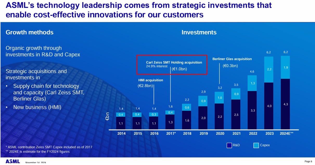

ASML is fundamentally an engineering-driven company, and this focus is deeply embedded in its culture. Their priority remains technical excellence rather than short-term financial optimization, much like Airbus. This engineering-centric culture minimizes time wasted on internal political considerations.
The Dutch culture, which values transparency and straightforwardness, enhances this efficiency by eliminating detours, unspoken words, and flattery. Though I am told by a friend it can be quite annoying as it can be quite rude more than straightforward sometimes.
In contrast, Japanese companies are often slowed down by internal political dynamics, which are influenced by their own corporate culture. This culture tends to prioritize harmony, seniority, and consensus, sometimes leading to slower decision-making and less flexibility in adapting to rapidly changing technological challenges.
Finally, ASML works closely with the Belgian institute IMEC, which has structured a European research ecosystem in semiconductors. In this sector, where expertise and interdependencies are numerous, this European network has given ASML a major competitive advantage by accelerating its technological advancements.
Structure of the lithography market
Today, high fixed costs and the need for constant investment in R&D (between 10 and 15% of revenue) make financial balance nearly impossible if a second player were to share the market.
In fact, Nikon and Canon did not attempt to compete with ASML on EUV, because the colossal investment would make no sense. ASML has several years of industrial expertise ahead.
To make such large-scale investments profitable, a competitor would need to capture market share, which would require:
Adapting all processes to the specifications of the new machines
Adapting other equipment to the characteristics of these machines
Even with market share, a new entrant could only make their investments profitable by capturing a very significant portion of the market. This remains highly unlikely.
In reality, Nikon and Canon’s only hope is to bet on the next technological breakthrough, one that will succeed EUV.
However, this possibility is not foreseeable in the next five years. Advances in EUV High-NA (or even Hyper-NA) still offer considerable room for improvement for ASML.
Lastly, ASML’s privileged relationship with foundries and designers like Nvidia makes any unexpected disruption very difficult.
Financial analysis
Since 2014, ASML has established itself as a true growth machine, showing an impressive increase of 370% over this period of its revenue, which equals an average revenue growth of 18% per year.
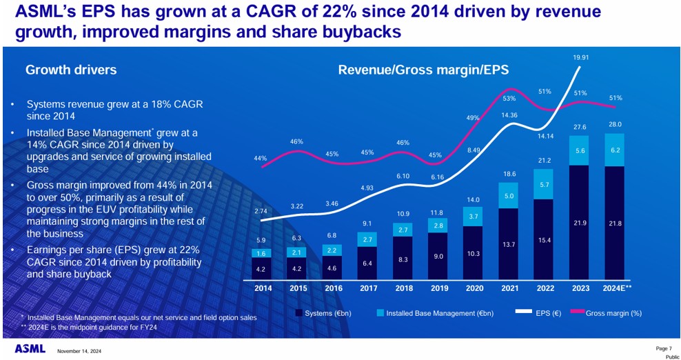

However, the market anticipated an acceleration of this trend, as seen in 2023. When that didn’t materialized in 2024 the stock tanked :
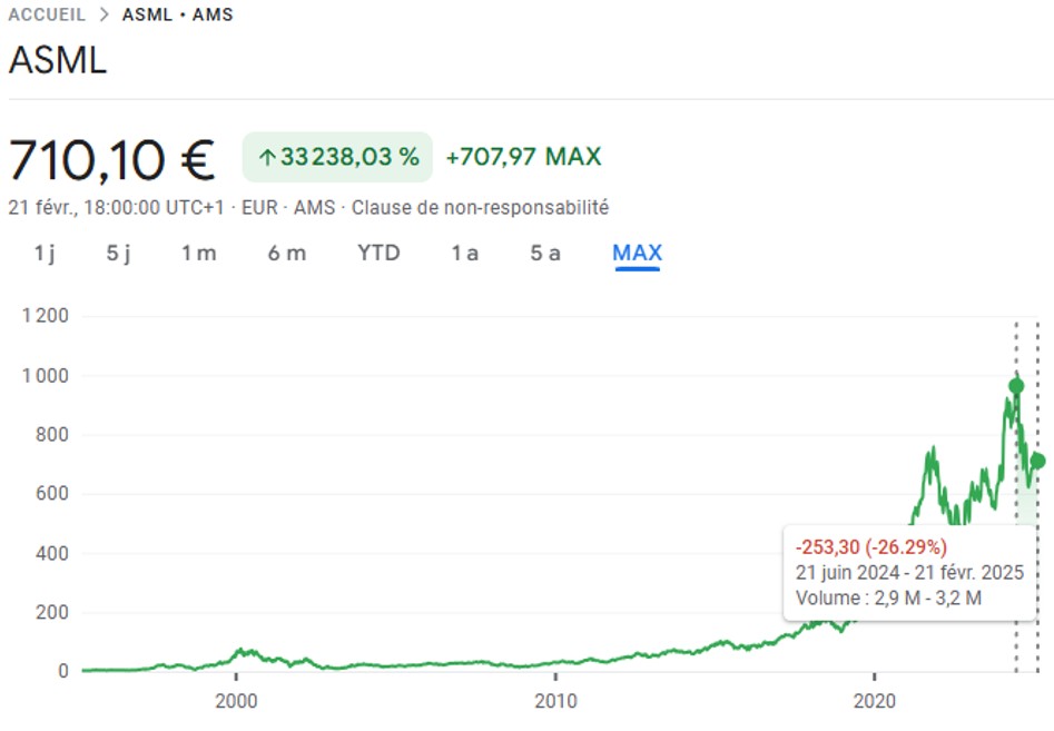
Though the long-term growth is still there.
Operating margin
ASML is a company that has seen its operating margin grow over the years, despite significant fluctuations. However, the trend is expected to continue upwards, potentially reaching 40% by 2028 with the ramp-up of its new “High EUV NA” machine.
But there may be challenges towards the adoption of that machine in the short-term, same as what happened with the Low NA equipment because of SCULTA equipment as we will see later.

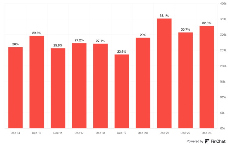
However, it seems difficult for ASML to achieve an operating margin higher than 42% given its current technologies. Moreover, It is better to take a cautious approach regarding the company’s outlook, as it is entirely possible that ASML will face additional challenges, including new restrictions or unforeseen delays from its clients.
Free Cash Flow

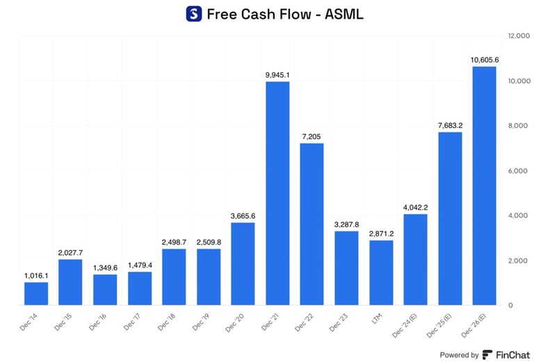
Regarding ASML, it’s unique because the semiconductor industry is cyclical, which means we are currently at a low point in terms of free cash flow before potentially seeing a significant rebound from clients who need to invest upstream to meet their customers’ needs.
It’s primarily the evolution of the operational cash flow that will influence the free cash flow, as ASML doesn’t need to increase its CAPEX to continue convincing its clients (at least for now).
Stock buybacks
In ASML’s case, I appreciate the fact that management only buys back shares when they believe the stock price is undervalued.
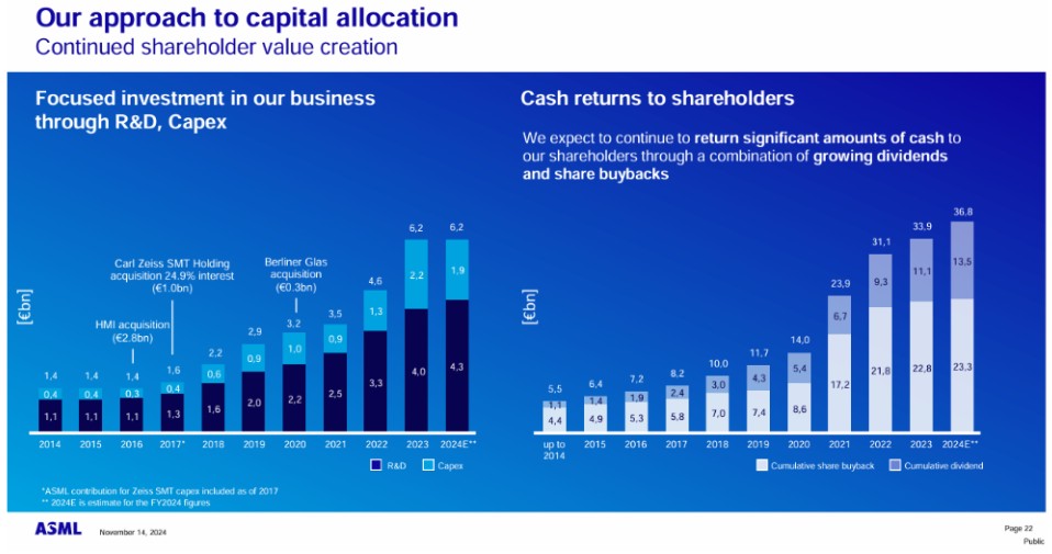
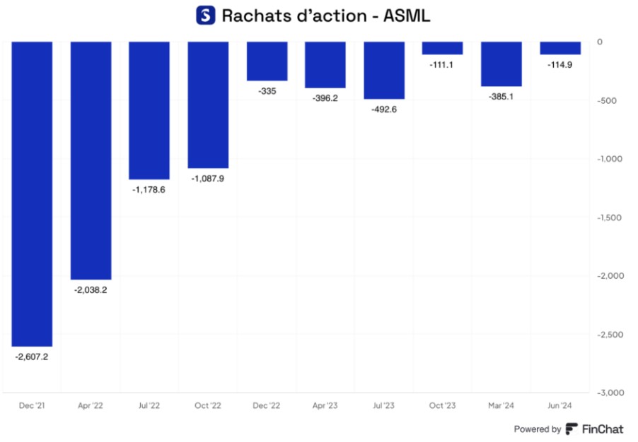
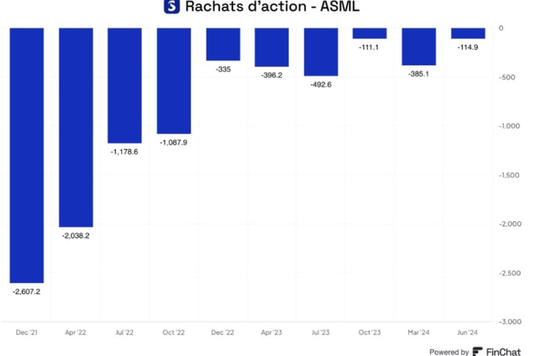
Thus, management conducted a massive share buyback in 2021 when the stock was trading around €450 to €500, considering it attractive.
However, as soon as the valuation levels became excessively high, the company quickly reduced its share repurchases.
Growth perspective
ASML also organizes Investor Days to share its forecasts. The most recent one took place in 2022, with the next scheduled for November 14, providing more updated information.
Here are the key perspectives shared during the 2022 Investor Day:
2025 Guidance: Revenue between €30 billion and €40 billion. As you know, this guidance was later revised to a range between €30 billion and €35 billion.
2030 Guidance: For the end of the decade, they are aiming for revenue between €44 billion and €60 billion.a
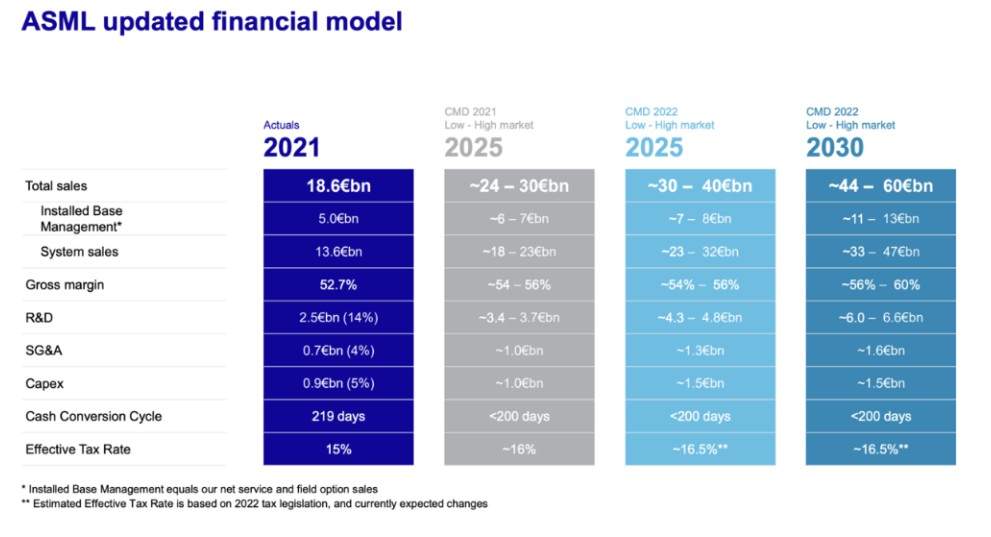
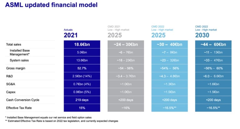
In the Investor day of 2024 they maintained their guidance :
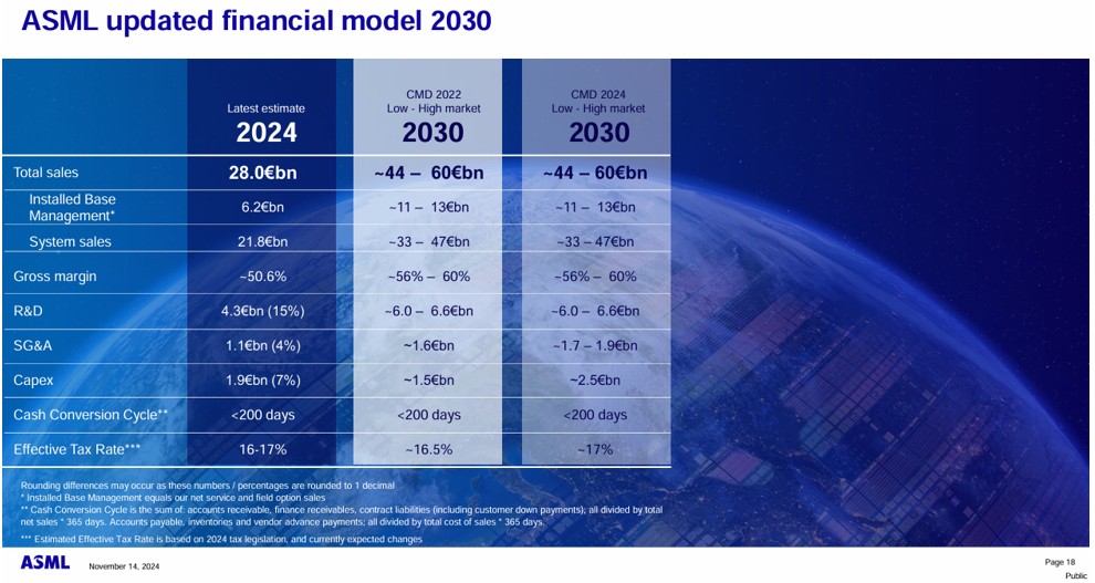
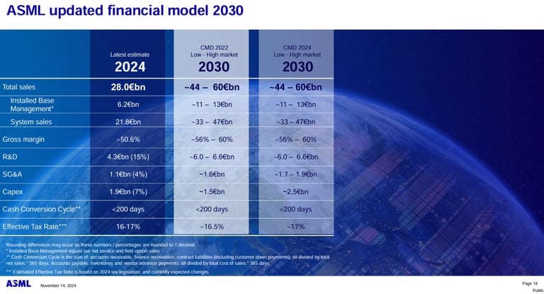
These forecasts are based on several scenarios.
Firstly, this scenario relies on strong growth in advanced logic chips, which have a minimum resolution of less than 28 nanometers, especially those under 7 nanometers. A lot of Nvidia’s chips fall into this category.
Production of advanced logic chips is expected to grow by 12% per year, compared to just 6.5% per year for all types of chips.

Is it possible to produce advanced Chips without EUV ?
I’ll make a brief digression because this point is important to understand.
Producing 7 nm chips with DUV lithography technologies is possible, but it comes at a cost. There are techniques called multi-patterning, where a wafer is passed multiple times under a lithography machine with different patterns. This allows the patterns to be stacked to reduce the minimum resolution size and helped push the limits before EUV arrived.
This technique is notably used by some foundries, like those in China, which are under sanctions for EUV machines but can still produce chips down to 7 nm.
However, as the resolution decreases, the number of multi-patterning steps must increase, going from 2 to 4. With each additional layer, productivity and yield are reduced due to a higher defect rate.
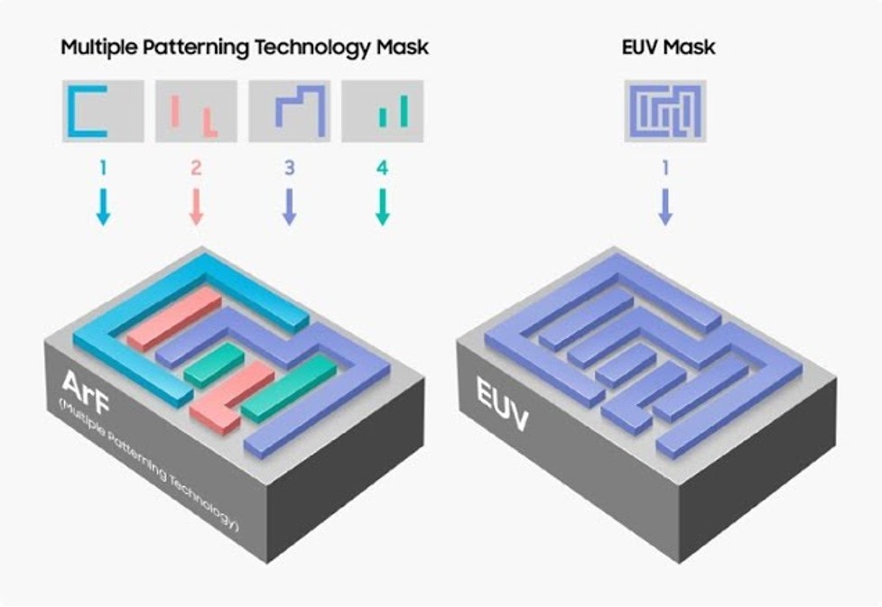
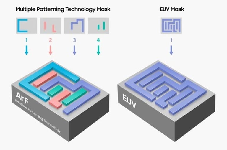
As a result, this significantly increases production costs. For example, producing a 7nm chip with minimal resolution costs 30% less, despite the system being much more expensive.
As complexity increases, it becomes less economically viable to rely solely on DUV technologies for chips with resolutions of 7 nanometers or less.
Finally, beyond reducing the minimum resolution, another avenue being used to increase transistor density and therefore the computing power of chips is advanced packaging.
I won’t go into detail, but the most promising technology right now is Hybrid Bonding, where BE Semiconductor is positioning itself as a leader.
A perspective on the need for EUV Equipment :
Let’s get back to the outlook.
The markets for the most advanced chips, whether logic or memory, will increasingly demand EUV technology, and eventually EUV High-NA.
In the graph below, we can already see that for logic chips smaller than 5 nm, it’s very difficult to do without EUV.
For memory chips, the need for EUV machines will also grow rapidly, though less than for DRAM and Advanced logic chips..
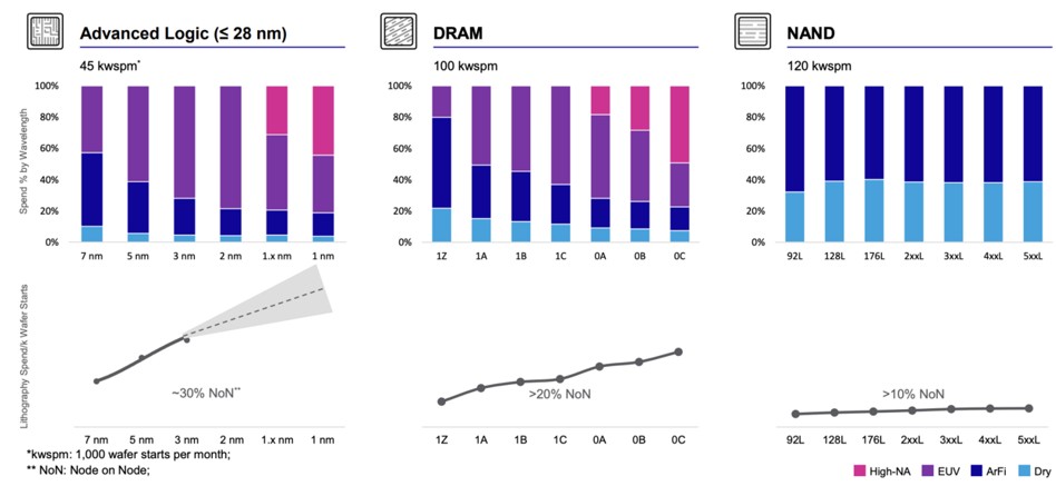
Of course, ASML also sells DUV machines, and that will remain a significant part of its business. However, due to their price, it is EUV, Low and High NA, that will drive ASML’s growth in the second half of the decade.
Also strong growth for DUV
Beyond these advanced chips, the vast majority of the market will remain in the “mature” chip sector.
This sector is also expected to grow significantly due to strong trends such as the energy transition, the electrification of economies, and empowering technologies that require many sensors (e.g., autonomous vehicles, autonomous robots, especially in logistics...).
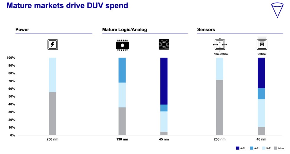
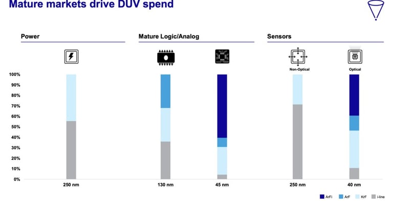
ASML is very well positioned to benefit from these megatrends, even though they may not require EUV. To remind you, in addition to producing the most advanced machines with EUV, they also make the most productive machines. No one offers exposure capacity in terms of wafers per hour as high, notably thanks to the breakthrough of the TWINSCAN, which has never been matched, as surprising as that may seem. I should still look more into it as that seems strange to me.
I think I might have found why they might have not been able to follow suite and replicate the design on short notice in FOCUS: The ASML Way :
« Immersion and the TwinScan turned out to be a match made in heaven. Making this 3D map is best done with a dry wafer, and with the TwinScan you could undertake the wet exposure while the next disc, still dry, was already being measured. Just like doing the dishes with an extra pair of hands. The tables of the TwinScan were driven by powerful motors, able to accelerate and decelerate in an instant. But directing the two simultaneously turned out to be far more complicated than imagined. The first TwinScan system ASML delivered in 2000 only carried the one wafer-table. It would need to wait some time for its sibling to arrive. A sophisticated name was spun to gloss things over: the TwinScan ‘Single’. But despite limping to market on one leg, ASML knew the machine would have no difficulty being sold. This new generation of lithography machines exposed wafers with a diameter of 300 millimeters, roughly the size of a vinyl record album. This was still a significant increase on the 200mm industry benchmark, allowing for more chips to be produced. Just like an album holds more songs than a single. »
Growth of services
Finally, ASML’s services are expected to continue growing with the increase in its installed base of machines. The more existing machines are upgraded, the more it creates demand for upgrades from clients who prefer to optimize their current equipment rather than buying the latest machine, often for cost reasons.
In 2022, management estimated an annual growth rate of 11 to 15% for this activity, which, as mentioned, is more profitable than selling machines.
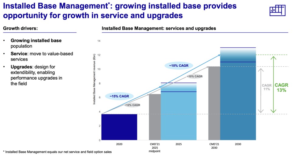
Synthesis of the growth perspective of ASML :
Thus, looking at the different segments of ASML’s business, I believe their 2030 guidance is definitely achievable. In the past, they have consistently exceeded their long-term guidance.
Therefore, from my perspective, they should be closer to the high end of the range, meaning between 52 and 60 billion euros in revenue by 2030, representing a growth of 11 to 14% per year.
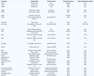
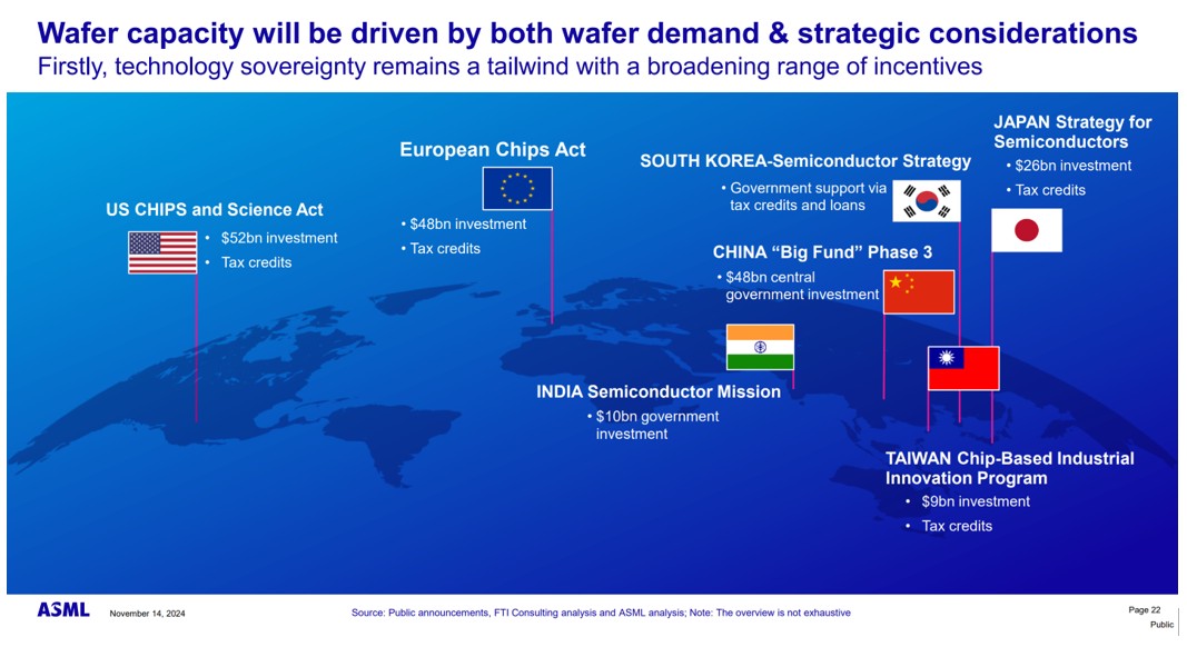
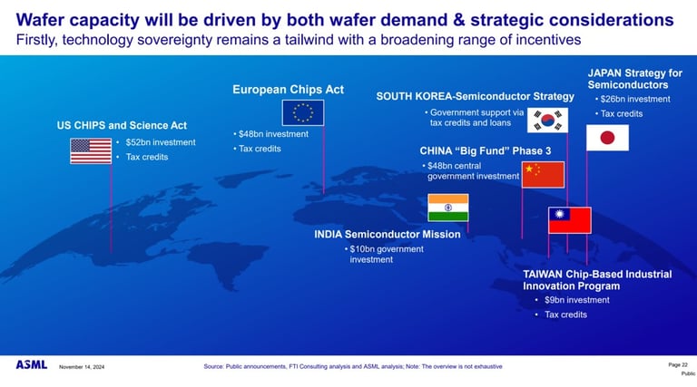
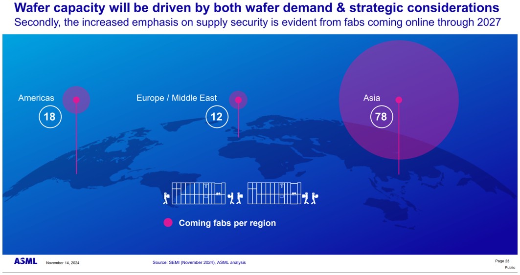
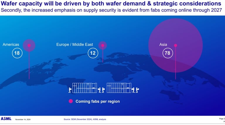
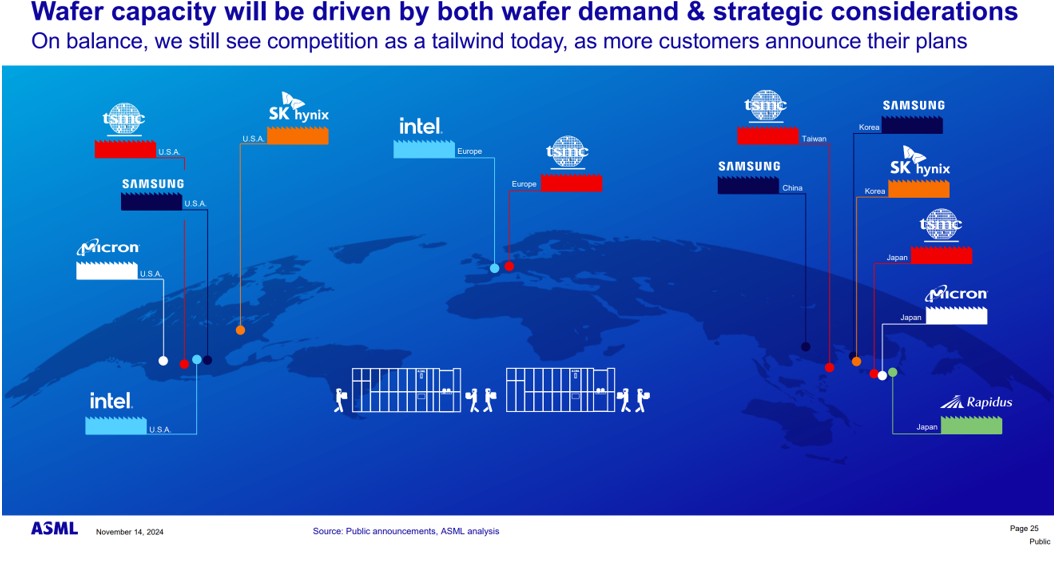
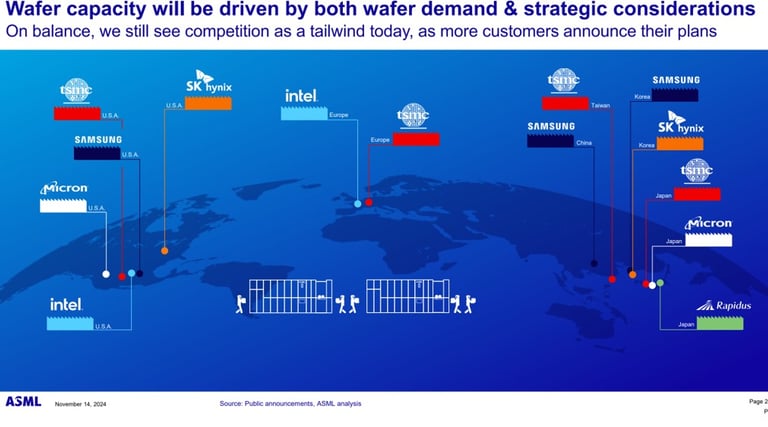
Risks
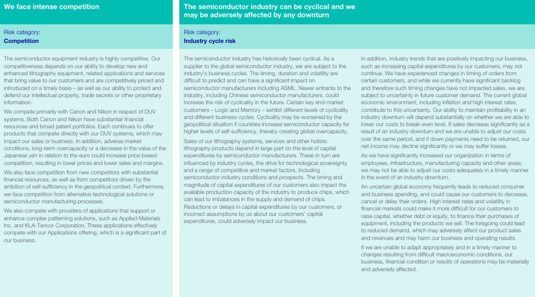
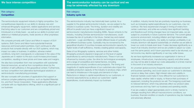
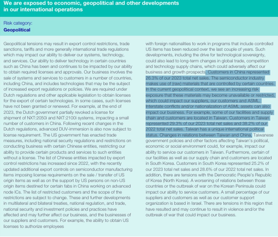
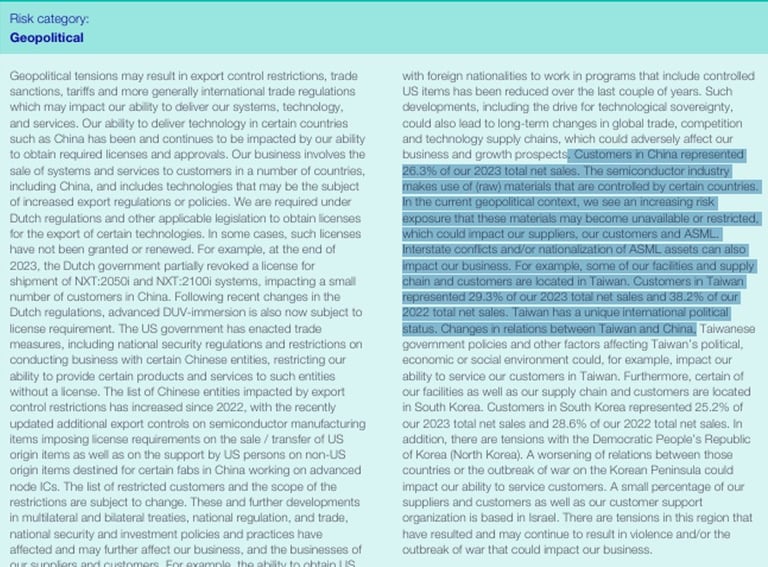
Regarding risks, two stand out particularly.
Technological Risk
The first risk, and probably the most significant in the long term, is the risk of technological disruption.
In the medium term, ASML is well-positioned, and as mentioned earlier, it is unlikely that they will be disrupted in their area of expertise in the near future. However, what has allowed ASML to dominate is its ability to anticipate and adopt innovations, such as the shift towards EUV technology. Therefore, it will be crucial for ASML to successfully navigate the next technological breakthrough to maintain its leadership position.
In my opinion, ASML’s competitive advantages, including its corporate culture and organizational structure, make it a strong candidate to remain technologically ahead in the lithography sector. However, it is not excluded that ASML's growth forecasts could be revised downward if advances in other technological fields reduce the need for lithography intensity.
For example, Applied Materials, the second-largest semiconductor equipment supplier in the world, introduced a new technology in 2023 called SCULPTA. This technology could potentially eliminate the need for double-patterning in EUV Low-NA machines, which would reduce demand for these machines. Which is what TSMC chose to do.
While it’s hard to quantify the impact of this technology at this stage, it is an evolution to watch closely, as it could have significant consequences on ASML's growth potential in the coming years
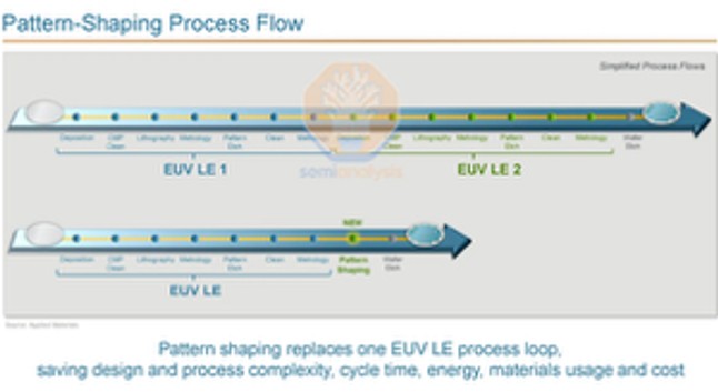
ASML is betting heavily on the development of High-NA technology to offer an alternative to Low-NA machines by reducing the need for double-patterning, thus undercutting SCULPTA.
It’s worth noting that Tokyo Electron also offers a competing solution to reduce the lithographic intensity of EUV.
The first High-NA machines have already been delivered to Intel, and management has confirmed that another customer will be delivered this quarter. However, this technology has not yet reached industrial production due to technical challenges, particularly limited productivity.
With a cost per machine of about 400 million euros, roughly 2.5 times the price of a Low-NA machine, manufacturers are exploring other options to improve resolution without investing in a technology that is still in the maturation phase.
The development of High-NA will be crucial for ASML in the medium term. TSMC, for example, has stated that it does not plan to adopt High-NA before at least 2026. This delay has contributed to the downward revision of ASML’s 2025 guidance.
However, advances in computational lithography allow for reasonable optimism regarding ASML’s ability to tackle these challenges. At NVIDIA’s 2023 GTC, a partnership between ASML, TSMC, Synopsis, and NVIDIA was announced to strengthen this field, which could accelerate the ability to overcome current challenges, particularly through Optical Proximity Correction (OPC).
Here is a link that shows quickly the technology :
https://www.youtube.com/watch?v=9RZreu5z_Gc
Computational lithography (and AI as well, I imagine) could enable faster development of upcoming lithography technologies in order to continue adhering to Moore's Law.
In summary, there are obviously technological risks for ASML, and it is impossible to invest in this stock long-term without paying attention to them. However, it is highly unlikely that this risk will have a significant impact in the medium term (of course, this depends on the valuation at which one buys).
Another competition could come from China that tries to duplicate the technology but here is what the CEO of ASML had to say on the subject on an interview :
“how far behind is China ? “
“here now, well, I think I think I've said that a few say few times publicly. I think, and a few people have said that China doesn't have access to EUV and EUV is critical for advanced logic chips. I think this has been demonstrated in the Western World? I go back again to the TSMC. In their story, uh, you know EUV was introduced for R&D around 2016-17. Started to go to production around 2018 and this means that China is at least I would say 10 years behind and most probably a bit more. Because as we were looking back in you know 16-17, they were already you know a couple of generation behind. So, you know 10-15 years is most probable, if you look at logic of where they stand and it's very very difficult to do Advanced logic without EUV. You can of course make a few chips over time, a few transistor but you cannot do it in volume. You cannot do it at a cost that is reasonable, so you cannot do it in a way that is economically viable. Taiwan is in the middle of this whole value chain. what how risky is that well I - I think that you know it's - it's a very difficult question I - you know I - I don't know to be honest because you can speculate on that, you can only have an opinion uh there's always a risk of course to- to have uh the supply chain concentrated in one place. I think no one can argue with that but then I would say we present a similar risk for the market. In this sense, you know guessing what's going to happen on geopolitics is difficult. Because anything happening with Taiwan will have major implication for the entire world, clearly. So, I'm not - I'm not one of the people who - who are very uh much looking at very bad scenario to Taiwan I think those are very unlikely but again that's more of a personal opinion than anything else. “
Now I think those were assumptions on China playing fair. So with some stealing of technology, I would not be surprised if they manage to do it in less than half the time estimated. But I think they still have at least an easy 5-year monopolistic position with the technology. Probably quite a bit more.
Update
The Chinese might be closer than ASML thinks or even I thought. I am still not worried because the Moat of ASML is strong enough even without a monopoly on the EUV technology but it’s still something to watch out for.
I will take 4-year with no competition at all for low NA EUV. I still take 4 years because it takes 2 and half years at least to train the support staff needed to learn how to maintain the complex EUV machines and as such they won’t have enough capacity to compete on ASML market at the start.
https://www.huaweicentral.com/huawei-is-allegedly-testing-china-made-euv-chip-making-machine/amp/
They say it will start to be in commercialization in 2026. Could be the case but let’s not forget it took ASML 10 more years than they thought it would take at the start also. Though, even if they manage to do it by 2026, there are other issues that they will have to confront.
First for EUV machines you have to pay them in the tens of millions or even hundreds of millions for the most advanced and thus you expect to use them for 10-15-20 years to produce chips. And you have to be sure that should there be an issue you can count on the maintenance personnel and upgrades that will come for those machines during that time.
Furthermore, with the trade restriction there was, ASML already didn’t sell EUV machines in china, only DUV ones. So, they wouldn’t lose market share in china even if the EUV machine are sold to SMIC (main china chip manufacturer).
Another point, is that the only customer of ASML that use EUV technology are : SAMSUNG, SK Hynix, Intel, TSMC and Micron.
I have a hard time seeing Intel, Micron and TSMC rely on china for the maintenance and upgrades of the heart of their fabs for obvious geopolitical reasons. As such, not worried about the Huawei manage to gain EUV technology for now.
Though in the very long term it might affect their margin a bit as it still competes with them on some machine (Low NA). So definitely something to watch out for.
Geopolitical Risks
The second risk for ASML is geopolitical.
The first aspect concerns a potential invasion of Taiwan by China. If such a scenario were to materialize, it would have a major impact on the semiconductor supply chain, but it is difficult to assess the precise consequences for ASML.
The second geopolitical aspect concerns export controls.
The United States has banned ASML from selling EUV machines to China. The U.S. government didn't even need to pressure the Dutch government. In fact, ASML relies on patents owned by the American consortium EUV LLC to produce its most advanced machines. Additionally, production depends on components supplied by American companies.
In practice, this situation does not change the overall demand for semiconductors, which remains high. If EUV machines cannot be sold to China, this demand could simply be redirected to other markets.
However, since September, ASML must also obtain export licenses for certain DUV machines, and this may have an impact in the medium term. However, this situation is already anticipated by Chinese players who heavily invested in ASML machines in 2023/2024.
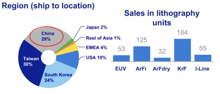

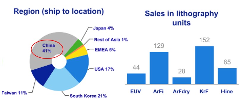
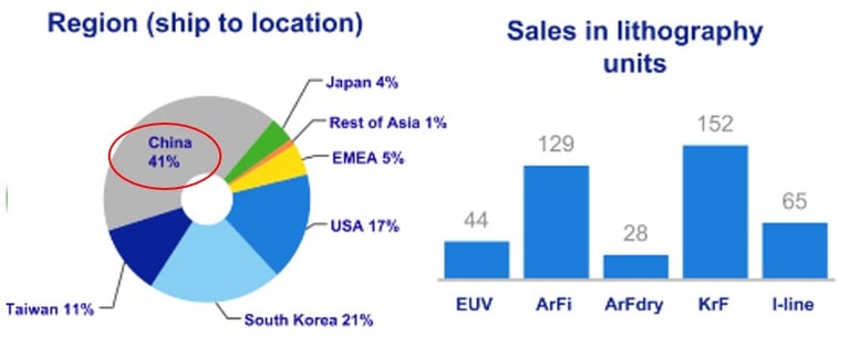
The geopolitical risk is certainly not to be excluded, but in my opinion, it creates more volatility than anything else. The real threat is the invasion of Taiwan, but in that case, ASML would not be the only one to suffer. And in the long term, I’m not sure it would change much, to be honest.
Because the demand would still be there for ASML, even bigger maybe, as you would need to rebuild factories as the demand would still be there. Though there would be an Impact on their results short to mid-term. It could actually a great buying opportunity as terrible as such an event would be for the world.
Legal risk
Nikon patent war may come back in 2029
Here is an extract of FOCUS : the ASML way on the subject
« Oerle, Zeelst, Meerveldhoven: nestled between these tongue-twisting tiny townships in the municipality of Veldhoven, a powerful monopoly was emerging. Years of investment in an improbable technology was yielding serious results, and in 2017 ASML reported over a billion euros in revenue from the new EUV machines. Meanwhile, ASML’s market share in conventional lithography systems had climbed to 90 percent. One company had been watching this rise through gritted teeth: Nikon. Right up until the ’90s, the Japanese technology group had been the market leader in lithography machines – until ASML came, saw and conquered. But there is still a way to turn things around when you’ve been kicked off the throne: sue the new king. In April 2017, Nikon initiated another patent lawsuit against ASML. To their dismay, Carl Zeiss SMT, the German lens maker’s semiconductor division, was also dragged in. The Japanese accused them of violating eleven patents in the Netherlands and filed simultaneous complaints in Germany and Japan. If the courts ruled in Nikon’s favor, ASML would have to cease the production of machines in Veldhoven. Once again, the survival of the company was at stake. Market leader or not, a looming ban on production was the last thing they needed. But this time, the attack did not come as a surprise. ASML still vividly remembered Nikon’s claims from 2001. That lawsuit came out of the blue and ended in 2004 with a so-called cross-licensing agreement. Nikon, ASML and Zeiss effectively signed a ceasefire so they could continue using each other’s technologies without being dragged to court. The deal cost ASML 87 million dollars and Zeiss had to pay Nikon another 58 million dollars. Part of the cross-licensing agreement expired in 2009, and when ASML reached out to discuss an extension, the Japanese were silent. In 2013, as the remaining agreements were about to expire, ASML knocked on Tokyo’s door again. Once again, Nikon didn’t respond. The Dutch were willing to pay a reasonable amount to continue the licenses, but Nikon wasn’t interested in an extension of the existing deal. It wanted a chunk of ASML’s revenue. In 2017, this amounted to more than 9 billion euros. Nikon was looking to receive potentially hundreds of millions of euros it would then be able to use to recoup its own lithography research costs. The Japanese EUV project had stalled in 2009, effectively gifting ASML a monopoly over these machines. A lingering resentment had simmered among the Japanese ever since: they had failed to win the first patent battle, and it had cost them their leading market position. Veldhoven, in turn, harbored a strong antipathy towards anything even remotely associated with the Japanese competition. You wouldn’t see the old-school ASML’ers with a Canon or Nikon camera. They would rather buy an Olympus or Sony – after all, Japan did produce the best cameras in the world. This gave Eric Maurice an idea – and a brilliant one, he might add. In 2011, two years before the Frenchman stepped down as CEO, he approached Martin van den Brink with a plan. As soon as the Japanese filed their first complaint about lithography machines, ASML should use camera patents to hit Nikon where it hurt the most. Meurice could feel the storm brewing, and he gave a stark warning to Van den Brink: ‘You’re gonna have a problem Martin, that’s why you need to attack them on their own turf. Make sure you get those patents.’ Van den Brink often clashed with Meurice, but he knew the Frenchman was clever. He took the warning to heart and consulted with Ton van Hoef, who managed ASML’s lithography patent portfolio. Patents needed to be acquired, and preferably not in plain sight. According to the database on company.info, in October 2011, a company called Tarsium B.V. was established. It was a shell company set up by ASML to stay under the radar of Nikon’s lawyers. On paper, Tarsium was officially registered in Amsterdam and in a residential area in Eindhoven. The name appeared to be derived from ‘tarsier’, the wide-eyed nocturnal primate native to islands of Southeast Asia that hunts insects under the cover of darkness. Between 2012 and 2014, Tarsium acquired nearly 10 million euros’ worth of patents for digital photography, including from Hewlett-Packard, Xerox, MediaTek, and the American patent aggregator Intellectual Ventures. The first patent, obtained in November 2012, described a method for selecting faces in an image. Convenient for quickly snapping a group shot. When the cross-licensing deal expired in 2014, ASML enlisted the help of Willem Hoyng, partner in Amsterdam-based law firm Hoyng Rokh Monegier and specialist in intellectual property. The conflict with Nikon became the biggest case of his fifty-year career. Hoyng quietly set about assembling a team of twenty lawyers, and for a time, everything remained calm. In 2015 and 2016, mediation attempts between ASML and Nikon once again failed, and the inevitable legal battle ensued. The new patent war had started, and as soon as Nikon fired its first shot on April 24, 2017, ASML deployed its secret weapon. On April 28, Tarsium transferred the accumulated patents to ASML and Zeiss, and on the same day, those companies sued Nikon. The outside world was surprised to hear the counterclaim also targeted cameras. Wasn’t this all about lithography? CEO Peter Wennink denied that Veldhoven was infringing on Japanese patents, explaining ASML’s counterclaim in a press release: ‘We have no other choice but to file these lawsuits. Nikon never took the negotiations seriously. We will defend ourselves with every means at our disposal.’ The lawsuits were beginning to stack up globally. But first, ASML had to defend itself against the Japanese allegations in the Netherlands. Willem Hoyng went to meet with Martin van den Brink. Right away, Martin asked him, ‘Ah, so you’re the famous lawyer – what chance do we have of winning these cases?’ Hoyng estimated perhaps as high as 80 percent. Van den Brink exploded. ‘We have more than fifteen cases going on. Have you calculated what 80 percent of 80 percent of 80 percent is? Keep going and I won’t be able to pay you by the end of it all. I want the fifteenth root of 80 percent! Until then you’ll be here every Friday afternoon to keep me up to date.’ And so nearly every Friday, just as requested, the lawyers met at ASML. Meetings with the intellectual property department took place first, followed by a mandatory brainstorming session in Van den Brink’s office. They figured it was not in Nikon’s interest to actually shut down ASML’s production: they just wanted money. A lot of it. But Martin van den Brink wasn’t about to let himself get cornered by a competitor. The Dutch judge saw the stack of cases on his desk grow by the day, filled with words like ‘onderdompelinglithografiebelichtingsinrichting’, the 46-letter Dutch word for an immersion lithography exposure device. Exasperated, he summoned the lawyers of both parties. If this was just about money, surely it could all be resolved a bit faster. He forced a discussion between Nikon and ASML, but Nikon had no intentions to negotiate: they wanted to win a case first so they could corner ASML and ask for more money. The subsequent meeting in San Francisco lasted less than two hours, and the lawyers were on a flight back to Amsterdam that same day. The first four of the Dutch patent cases ruled in favor of ASML and Zeiss. But this was no cause for celebration. The company was on the line with every case: lose just one of the next hearings and they would lose everything. Zeiss, now fully intertwined with ASML, was the most concerned. The companies were united in their legal battle against Nikon, but they were dependent on the tempo of the court, which was progressing at a snail’s pace, according to Van den Brink. In a patent dispute, you need momentum to force a breakthrough. A year and half later, the breakthrough finally came. In August 2018, the American International Trade Commission ruled that Nikon had infringed upon the camera patents owned by ASML and Zeiss. Suddenly, Nikon’s camera division was facing an American import ban, and the Japanese were getting nervous. As the complaining party to the ITC, ASML and Zeiss had to demonstrate that they were suffering real economic damage, which meant there needed to be a camera available for sale in the US that used the patented parts. To everyone’s surprise, in the fall of 2018, Zeiss announced the ZX1. It was a compact digital camera with a fixed lens and large touchscreen: jet black, angular, with built-in photo editing software and internet connection. There was even a catchy slogan: ‘Shoot, Edit, Share’. The industry press was perplexed. When Zeiss had last made cameras, they still required roll film. Digital camera sales had plummeted since the iPhone’s arrival, with most people just using their phones to take photos. Was Zeiss seriously planning on entering this declining market now? Zeiss promised the ZX1 would be available in early 2019 – although they refused to reveal the price. A team from the American division built some prototypes, and Zeiss announced the ZX1 at the Photokina fair in Frankfurt. It was a grand affair, with the employees welcoming the gathered media with applause. It was like the world had been turned upside down. In December, a YouTube video appeared featuring a German photographer trying out the ZX1 for the first time, taking snapshots while wandering around the sushi shops in the Little Tokyo district of Düsseldorf. Another jab at the Japanese. Nikon became concerned. With four lost cases and a threat from the ITC to their name, the Japanese buckled and decided they wanted to negotiate a new agreement at a more reasonable rate. The parties were brought together by Edward Infante, the American judge who handled the previous confrontation between Nikon and ASML. On January 23, 2019, Nikon, ASML, and Carl Zeiss released a joint statement to the press: the deal was done. The Germans and Dutch paid Nikon 150 million euro (of which ASML paid 131 million) for the use of their patents until 2029, and ASML had to cover a 0.8 percent royalty on every immersion machine sold. It was a fraction of the percentage Nikon originally demanded. In retrospect, Nikon overestimated its own position. When you put smart engineers in two companies that develop the same product, the same ideas can easily emerge. Many of the patents Nikon gathered were granted too effortlessly by the European patent office, but it was undeniably the psychological blow of the camera patents that secured the knockout. In October 2019, the shell company Tarsium disappeared from the face of the earth. And what came of the ZX1, with its ‘Shoot, Edit, Share’? A handful of prototypes landed in the hands of reviewers. A few videos and blogs praised the metal lens cap and silent shutter, as well as the included shoulder strap. But they all wondered the same thing: when would the camera finally be available for purchase? For a brief moment in October 2020, it seemed like it could be ordered from an American online store for a mere 6000 dollars. However, the ZX1 was never actually sold, let alone delivered. When photographers enquired about it, Zeiss’ official response was: ‘We are very critical about the finetuning of all aspects of our camera.’ And that is where it ended. In 2020, Zeiss referred to the ZX1 as a ‘concept camera’. As if it had never existed, as if it had only been built to make Nikon’s life difficult. But the ZX1 didn’t leave without a trace. Back in his office, Martin van den Brink rummages through his awards and other memorabilia to retrieve a white box. A name is embossed on the front: Zeiss ZX1 – still wrapped in plastic, with the manual untouched. He holds the camera up to his eye and grins. ‘Brand-new. No idea if it even works – I’ve never taken a photo with it myself.’ »
GOVERNANCE
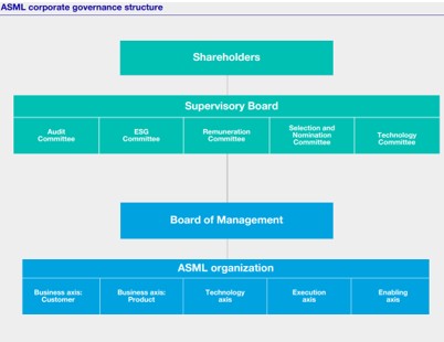
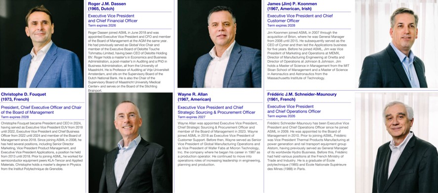
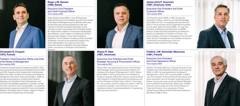
The CEO is not the founder but has been In ASML’s business for nearly 20 years, so it is fair to assume that he knows and understand ASML’s business well. He has also worked before ASML at ASML’s competitor KLA and Applied Materials, so he knows the industry well.
The other members seem to also nearly all have experience in the industry and they have been here through ASML’s success and good returns.
Though there is a concern to have on the fact that Peter wennink and Martin van den brick have both retired and have been pillars for the company for a long time. ASML is entering in a new phase of leadership. We will have to watch how the new leadership perform.
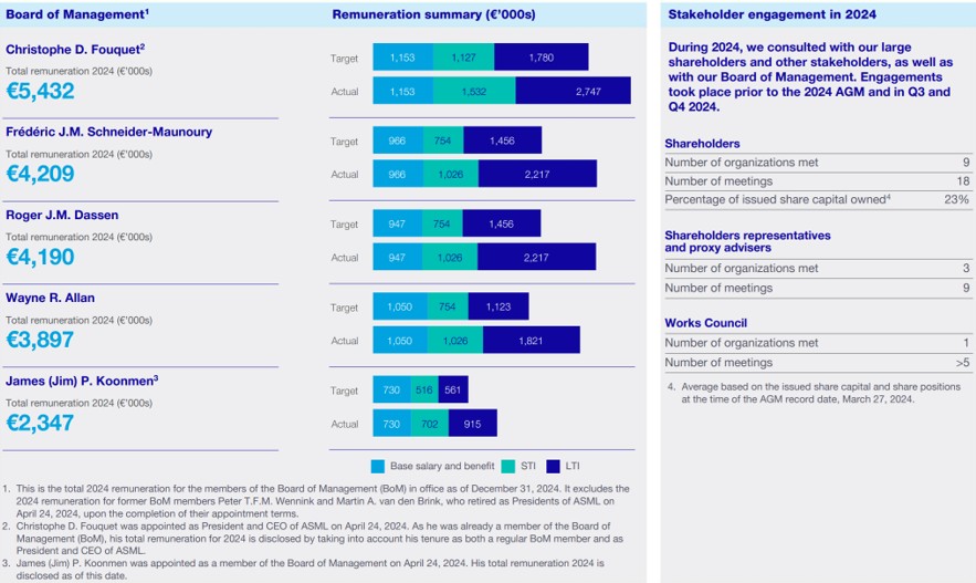
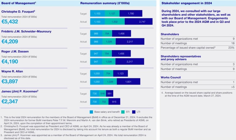
I like that the biggest part of their remuneration is on LTI 🡪 long-term criteria
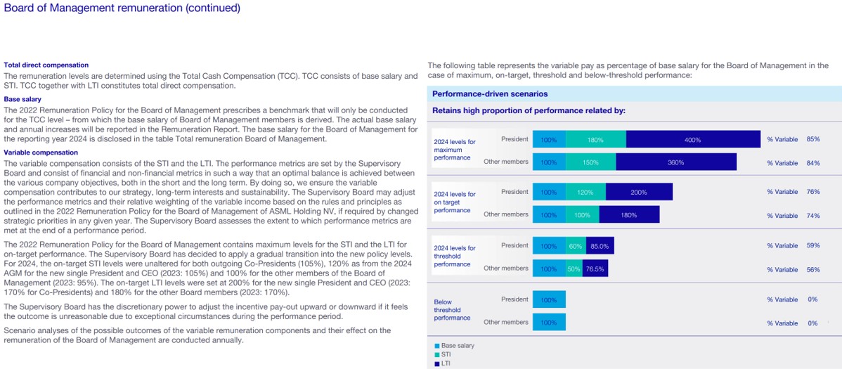

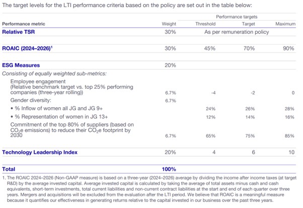
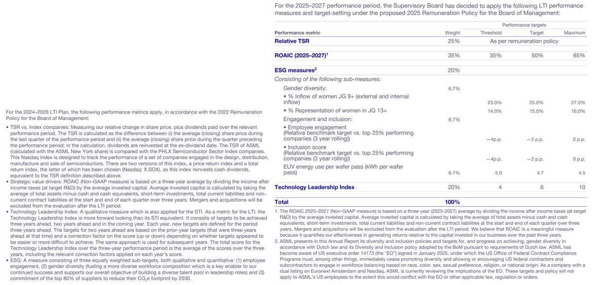
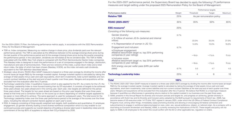
I don’t like the “TSR vs Index companies” criteria as I would prefer a fundamental criteria than a criteria based on share price, as it could incentive the management to do share buybacks at not such a good price to just increase the price of the stock without thinking about the long-term of the company.
I would rather that they increase the share based on ROAIC and Technology Leadership Index as I feel it is more important for the business long-term.
But as they still have a good history on doing buybacks at reasonable price and the share of that compensation decreased in 2025 for the benefit of ROAIC, I am not too concerned about it for now. But still something to watch.
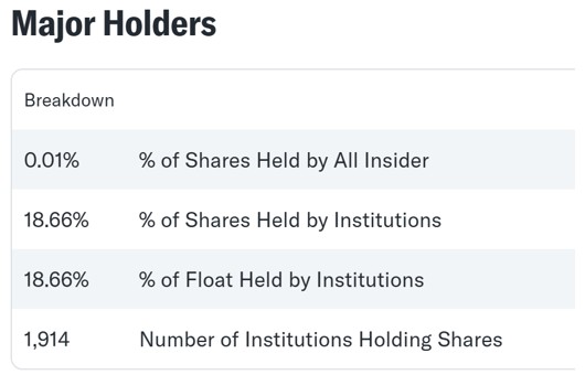

From TSMC earning call transcript :
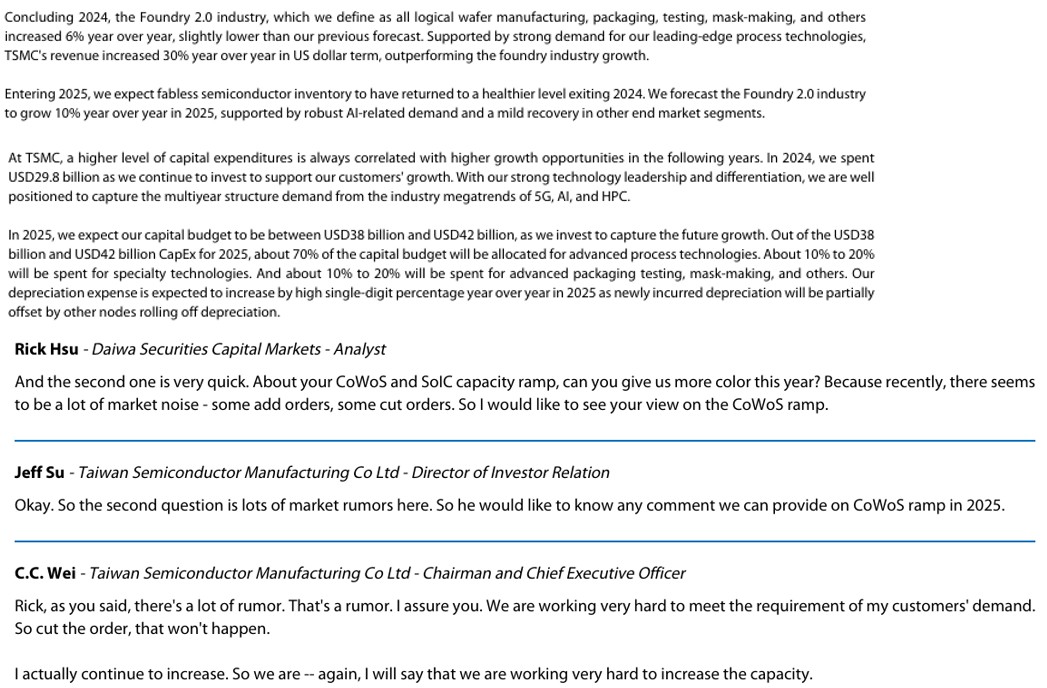

More CAPEX from TSMC to build new plants and equip them seems to be on the cards which means more money spent on ASML’s equipment.

As TSMC need to produce smaller and smaller chips they will need more of ASML’s equipment.

That seems like a bold claim and prediction 40% CAGR for the next 5 years, it’s great and amazing for ASML if it happens. But I don’t need it to necessarily be true. As long as TSMC act on that plan and expand their capacities and thus buy more of ASML’s lithography machine. Though we should keep in mind it could mean that there could be an overcapacity at some point if the demand for AI slows at some point.
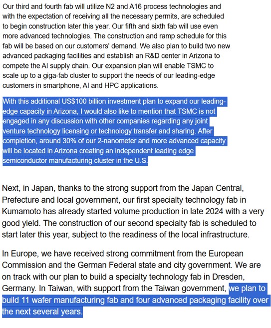
They seem to be on a full-on capex expansion. Which is great news for ASML. Though if AI doesn’t bring revenue for the hyperscaler at some point the demand might slow at some point, always something to keep in mind. Semiconductor is cyclical industry historicaly, so we might have growth for the AI sector for the next 2 years maybe but it could sharply lower if there is overcapacity.
Valuation & Conclusion
In conclusion, ASML is, for me, one of the finest companies in the world, operating in a strategic industry.
Semiconductors are the "oil of the 21st century," powering sectors such as automotive, defense, technology, cloud computing, and AI, and ASML is indispensable in producing the most advanced chips.
Its monopoly position in EUV lithography, coupled with its unique competitive advantages, makes this leadership almost unassailable for quite some time.
ASML is surely a great business, and fulfills the key investing framework which is: "in a gold
rush, invest in picks and shovels". ASML sells the machinery necessary to build all related to
the AI gold rush, and therefore is the picks and shovels investment opportunity.
Today, it is my strongest conviction in Europe, and it is fortunate that this company is eligible for the PEA (Plan d'Épargne en Actions).
Of course, volatility is high, particularly due to geopolitical risks and sometimes excessive valuation levels, amplified by the AI hype.
Such a valuation means that ASML cannot afford to make mistakes, and short-term disappointments like the last quarters can lead to significant fluctuations.
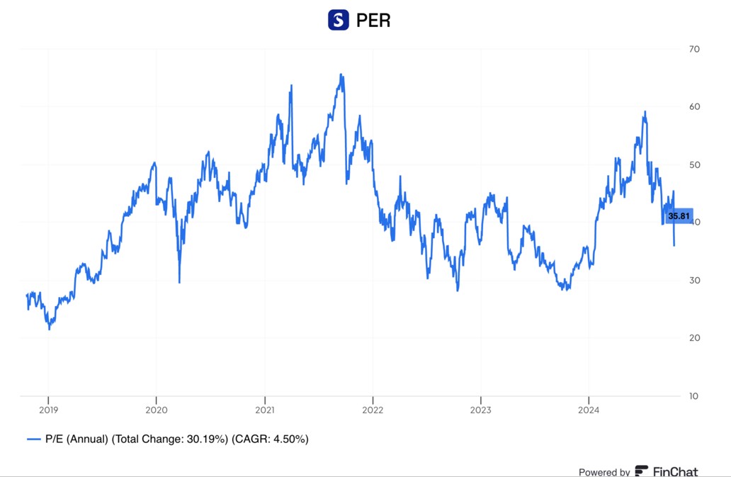
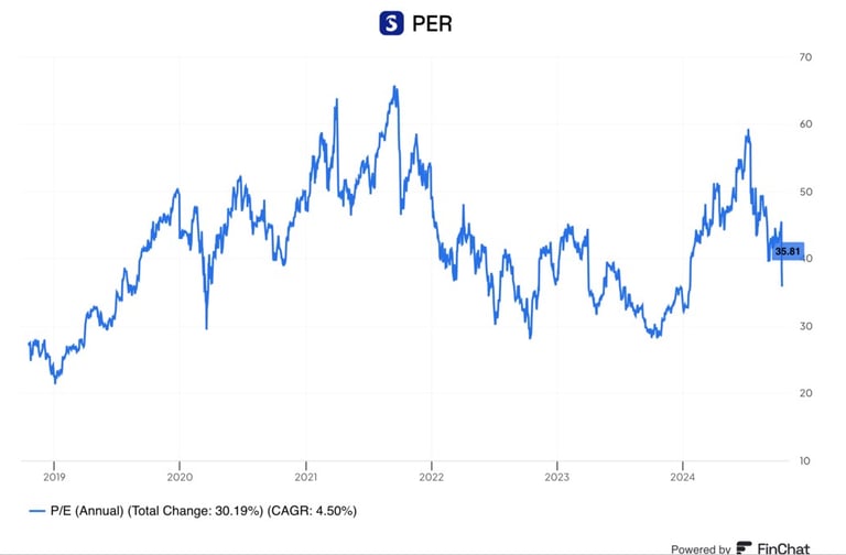
With ASML’s Guidance, Revenues for 2023 and 2024 were around 28 billion, the outlook is for growth to 30 or 35 billion EUR in revenues.
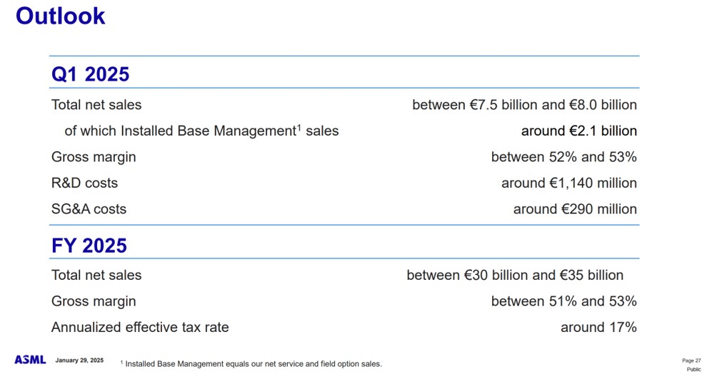
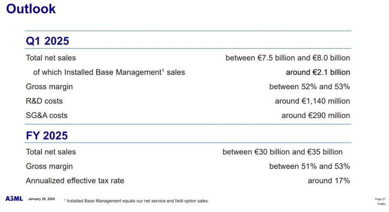
If we look at consensus Wall Street estimates for ASML, the earnings growth going forward is expected to be in line with the revenue growth and around 20%.
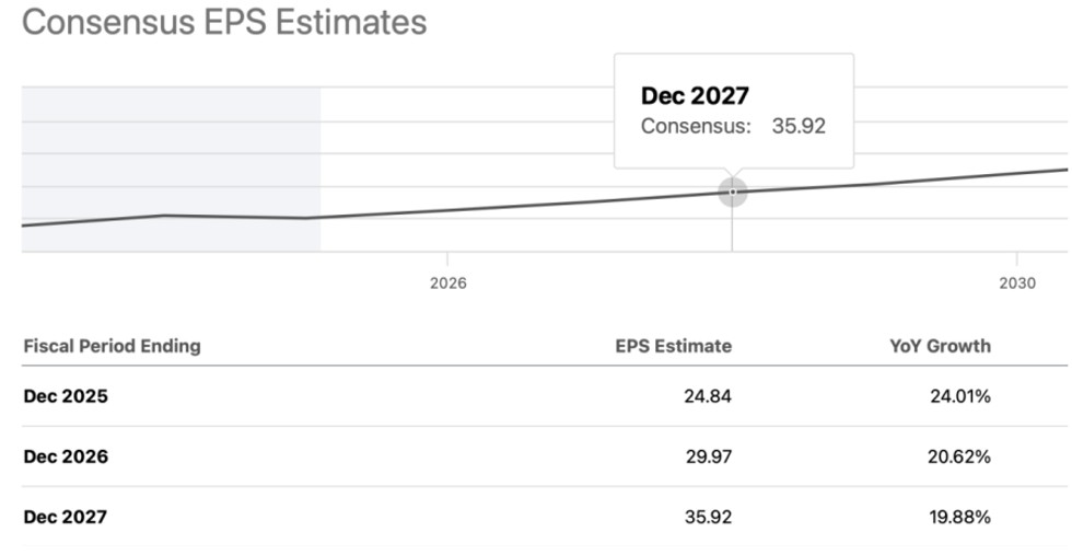
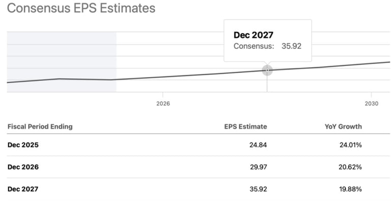
One can debate whether the current PE ratio of 37 is high or low for expected 20% earnings growth, which then also explains the volatility of the stock, where small changes in growth expectations, affect also the valuation, and result in big changes in the stock price.
2030 guidance :
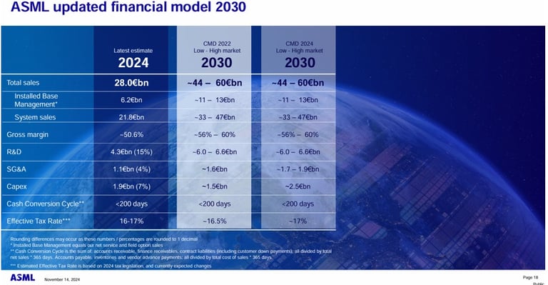
For example, let's take the 36 EUR EPS estimate for 2027, if the growth is just a bit slower than expected, and the EPS is 30 EUR, where the market applies a 30 PE ratio to it, ASML's stock price in 2027 could be 900 EUR. However, if the growth is better than consensus, let's say EPS of 40 EUR, with a PE ratio of 40, the stock price can go to 1600 EUR. Whether EPS will be 30 or 40 will depend on many factors, from the economy, the rate of growth in the industry in 2027 etc.
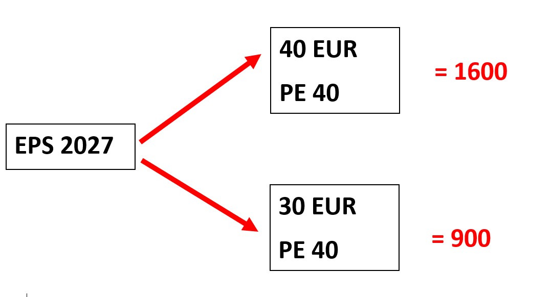
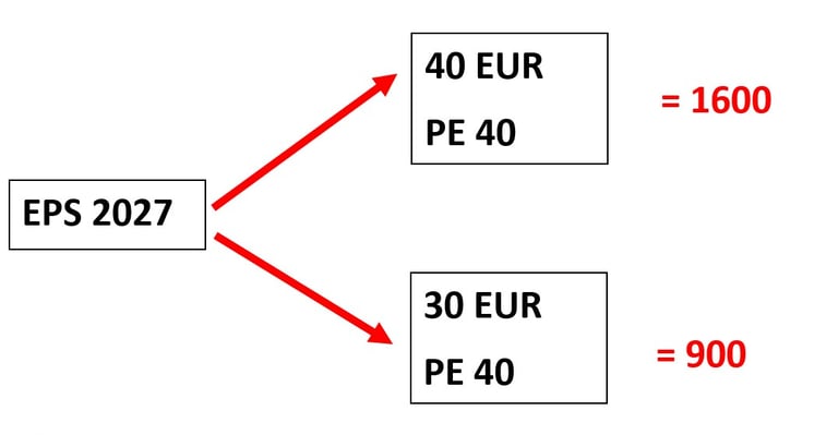
If we take Wall Street's estimates, the range for 2026 EPS is between 21.55 EUR and 32.96 EUR.
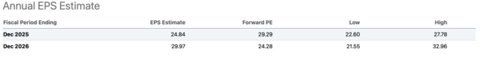
In the bad-case scenario, that can be due to sanctions, possible long-term competition arising as that is something often happening as a consequence of sanctions, or some other factors, with EPS of 22 in 2026, and a PE ratio of 20 on some currently unknown future weakness, I am looking at a stock price of 440 EUR. A price on which I would just increase my current position as it would be priced for a bad future.
SO, as discussed above, comparing an unlikely downside of 440 to the possible upside to 1600
on growth, ASML offers a positive risk and reward scenario in my opinion.
With 2030 CEO’s outlook :
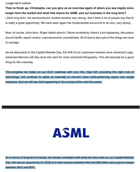
Expected revenues for 2030 are between 44 and 60 billion EUR. Consequently, we can expect earnings to be between 15 and 22 billion. Thus, in a very bad case scenario, with lower growth expectations, a valuation of 15 on 15 billion EUR, the market capitalization in 2030 could be 225 billion EUR. (it is 262 Billion now)
On the positive side, with 22 billion of profits and a valuation of 30, the market capitalization could be 660 billion for almost a 3x, if not more.
To conclude, ASML stock offers a very positive risk and reward situation, where if things go bad, it is likely one will not lose much money. However, if things go well, it is still possible to get a 3X to 4x return from ASML stock now.
But as said before there are still risks with this investment and it is one that one has to follow as it is a complex one.
© 2025-2026. All rights reserved.
Centro Research
info@centroresearch.eu
Investment research of securities and markets
Reports and other shared materials should not constitute as financial advice. Investment decisions require individual due diligence and one should seek qualified counsel.